
Abstract
We present a new result for the wavelength-selective characteristics of a 1D photonic microcavity based on porous silicon. These properties are studied in both experimentation and simulation. The 1D Fabry–Perot cavity is fabricated by the electrochemical etching of a low-resistivity silicon wafer with modulation of applied current densities. The simulation relies on the transfer matrix method (TMM) to design and predict the optical properties of a 1D photonic microcavity as well as the relation between anodization parameters with reflection spectra. The experimental results show that the elaborated porous silicon photonic microcavities have the wavelength-selective property in a controllable range of 550–775 nm. We have grown cavity structures of 20 stacked layers and the line width at full-width half-maximum (FWHM) of the transmission band of cavity is 20 nm, centered at 643.27 nm. Measured spectral characteristics of photonic microcavity agree with the simulation results.
Export citation and abstract BibTeX RIS

Content from this work may be used under the terms of the Creative Commons Attribution-NonCommercial-ShareAlike 3.0 licence. Any further distribution of this work must maintain attribution to the author(s) and the title of the work, journal citation and DOI.
1. Introduction
In recent years, porous silicon (PS) has generated great interest in photonic crystal and sensor devices. PS is a unique material that can provide the link between silicon technology and optoelectronic devices because it is inherently silicon-based, therefore the device integration into a standard microelectronics platform is facilitated, and it is porous, so that tuning its optical properties is possible. In the porous structure, PS consists of many pores and silicon residuals and can usually be described as a homogeneous mixture of silicon, air and, eventually, silicon dioxide. Based on porosity, PS can be classified into three types: nano-, meso- and macro-pores. In the case of PS nano- and meso-pores, the size of both the silicon residuals and the air voids (pores) can be in the range of a few to tens of nanometers. Since light has sub-micrometer wavelengths, PS can be optically described in the light range as an 'effective medium' [1], whose optical properties mainly depend on the relative content of silicon and air (i.e. porosity). The 1D photonic crystal based on PS multilayers is possible because [2] (i) the etching process is self-limited (i.e. once a porous layer is formed, the electrochemical etching of this layer stops); (ii) the etching occurs mainly in correspondence with the pores; (iii) the porosity depends only on the current density once the other etching parameters are kept fixed; and (iv) the refractive index of PS depends on its porosity. Therefore, by varying the applied current density during the etching process, it is possible to vary the porosity in the etching direction. In this way, a stack of PS layers of different porosities (and hence different refractive indices) forms a dielectric multilayer. Depending on the structure as well as the number of layers, the stack can act as an optical interference filter [3, 4], waveguide [5], omni-directional mirror [6], rugate filter [7] or microcavity [8, 9]. The structure of the microcavity, also called a Fabry–Perot filter, consists of two parallel distributed Bragg reflectors (DBRs) separated by a spacer layer, whose reflective index can be the same as or different from the ones used for the DBRs. The optical thickness of the spacer layer can be λ or λ/2 [10]. The reflectivity spectrum of this structured material is characterized by a narrow pass-band centered in a high reflectivity wavelength range. Microcavities can be used as band-pass filters with a tuned position of the peak [2, 11], tunable mirrors [12] and highly sensible detectors of substances like ethanol, methanol, acetone, chlorobenzene and nitrogen dioxide [13–16]. They have also been used for optical biosensors and chemical sensor fabrication.
In this work, we investigate the wavelength-selective characteristics of a 1D photonic crystal based on a PS multilayer designed as a microcavity. Before fabricating the microcavity, a simulation program based on the transfer matrix method (TMM) was set up in order to design and predict the optical properties of a microcavity. The elaborated microcavity has wavelength selective properties in the range from 550 to 775 nm, and its reflectivity is about 70−80%. The spectral and structural characteristics of the microcavity have been compared with the simulation results.
2. Simulation on 1D photonic microcavity
A simulation program based on the TMM has been realized on wave transmission in a one-dimensional structure. We consider a 1D photonic crystal structure consisting of alternating nano-PS layers of different refractive indices coupled to a homogeneous medium characterized by refractive index n0 at the initial medium and n s at final medium. n H and n L are the layer's refractive indices, d H and d L are the thicknesses of the nano-PS layers, and Λ is the period of the 1D structure (Λ=d H +d L ). The configuration of the 1D microcavity is shown in figure 1. A(x) represents the amplitude of the right-traveling-wave and B(x) that of the left-traveling wave. In addition, because A(x) and B(x) are not continuous at the interfaces due to the reflection, there are four different plane waves Am (x), A'm (x), Bm (x) andB'm (x) in each layer (see figure 1). If the amplitudes Am and Bm of the plane waves at interface x=xm are presented as column vectors, the plane waves on different layers can be related by [17]

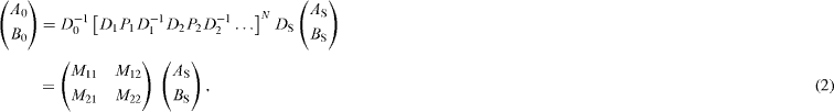
where m=1, 2, 3...,2N+1. The relation between A0, B0 and A S , B S can thus be written as
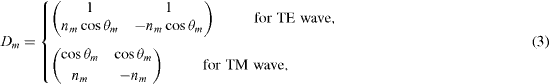
where N is the number of periods in the structure, Dm are the dynamical matrices given by
and Pm is the propagation matrix that can be written as

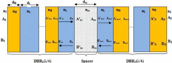
Figure 1 Schematic cross section of a 1D microcavity. n ss and d ss are the refractive index and thickness of the spacer layer, respectively. This spacer is inserted between two symmetric DBRs with refractive indices n H and n L and thicknesses d H and d L .
If the light is incident from lossless medium n0 , the reflectance can be calculated as

where R is the reflective coefficient.
Based on the above-mentioned theory, we set up a program for the simulation of filter structure in the visible region by using Matlab software. To simulate the microcavity, we only changed equation (
The simulation program contains the following parameters: (i) refractive index of ambient medium (n0); (ii) refractive index of substrate (n s ); (iii) incidence angle (θ); (iv) number of layers (N) in the 1D nano-PS multilayer; (v) refractive indices (nm ); (vi) thickness (dm ) of periodic layers; (vii) wavelength λ varied from the initial to the final values of the reflective wavelength; and (viii) thickness of the spacer (d ss ) and refractive index of spacer layer (n ss ).
Figure 2 shows the calculated reflection spectrum of the 1D microcavity with 20 stack layers having a refractive ratio of n H /n L =2.5/1.55. The thickness of one layer has been calculated to obtain a resonant wavelength at 650 nm.

Figure 2 Simulated reflection spectrum of a 1D photonic microcavity with wavelength resonance at λ0=650 nm. The ratio of n H /n L is 2.5/1.55 and d ss =λ0/2 n s .
Figure 3 shows the influence of the refractive index of the spacer layer, which was sandwiched between DBR mirrors, on the reflection spectrum of a 1D photonic microcavity. The λ/4-DBRs that form the microcavity have n L =1.55, n H =2.5 and stack-layer number N=4.
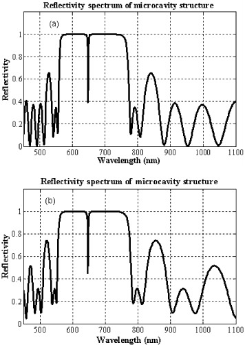
Figure 3 Reflection spectrum of a microcavity consisting of two DBRs with n L =1.55 and n H =2.5. The thickness of the spacer layer is d ss =λ/2n ss and its refractive index n ss is 1.4 (a) and 2.5 (b), respectively.
The calculation has been made for two possible cases, such as refractive index n s lower than n L (n ss =1.4), and equal to n H (n ss =2.5), respectively. The transmission peak that is positioned at 650 nm does not change and its reflectivity at cavity-resonant wavelength is almost zero for two cases. The difference between these spectra is observed at the side-lobes only.
The dependence of the line width of the transmission band on the number N of periods of the DBRs is shown in figure 4. When N increases from 2 to 8, the line width of the band-pass decreases from 18 to 0.2 nm, the reflectivity of the band-gap increases up to 100% and its edges become sharper.
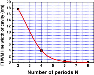
Figure 4 Simulation results of band-pass line width of microcavities with resonant wavelength at 650 nm when the DBRs have a different number of periods.
3. Experimental setup
A 1D photonic porous silicon microcavity (1D-PPSM) has been formed by electrochemical etching of highly doped p-type silicon wafers (resistivity is 0.01−0.1 Ωcm) in an aqueous HF:ethanol electrolyte. The p-type silicon substrates yield the most favorable porous silicon morphology. The pores are large enough to allow infiltration of other species, but interconnected and small enough to allow porous silicon to be treated as an effective medium for visible and infrared light [18]. The electrolyte with a concentration of 16% HF and ethanol of ratio 1 : 2, respectively, is chosen because of the large porosity variation obtained by varying the applied current. The computer-controlled Galvanostat was used for the electrochemical process, so precise control over the current density and etching time were achieved, and this results in good control of the refractive index and thickness over the individual layers of the multilayer structure. A porous silicon microcavity is formed by first etching a top DBR with alternating λ/4-thickness layers of low and high porosities (high and low refractive indices, respectively) by applying the periodically varied current density J1=15 mA cm −2 for 4.76 s and J2=50 mA cm −2 for 2.86 s, then etching a λ/2-wavelength thickness spacer layer with the same refractive index as the high porosity mirror layers with J2=50 mA cm −2 for 5.71 s, and finally etching a bottom DBR with the same conditions as the top one. The detailed electrochemical etching conditions are presented in table 1.
Table 1. Electrochemical etching condition for a porous silicon microcavity.
| DBR on top | 15 | 4.76 |
| (4.5 periods) | 50 | 2.86 |
| Spacer layer | 50 | 5.71 |
| (1 period) | ||
| DBR on bottom | 15 | 4.76 |
| (5 periods) | 50 | 2.86 |
The porous silicon microcavity used in our cases typically consists of a 4.5/5 period upper/lower DBR. Each period has one pair of low and high porosity layers. Therefore, a half period means that there is an additional low porosity layer formed. The PS microcavity was rinsed in methanol and isopropanol after anodization and dried in nitrogen ambient. The nano- and micro-structural characteristics of the PS microcavity was determined by field-emission scanning electron microscopy (FE-SEM; S-4800) and the reflectance spectra of samples were studied by a UV–VIS–NIR spectrophotometer (Varian Cary-5000).
4. Results and discussion
The nano- and micro-structures of the prepared 1D photonic crystal were analyzed by using FE-SEM.
In FE-SEM images, the dark region is air and the light region is silicon in the skeleton form. It can be observed in figure 5(a) that the FE-SEM image shows different gray levels depending on the porosity of the layers. Based on this difference, the layers of the stack are distinguished and therefore the thickness of the spacer can be determined as about 180 nm (the refractive index of the spacer layer is about 1.8). As seen in figure 5(b), the typical sizes of the silicon residuals and air voices are less than 50 nm.
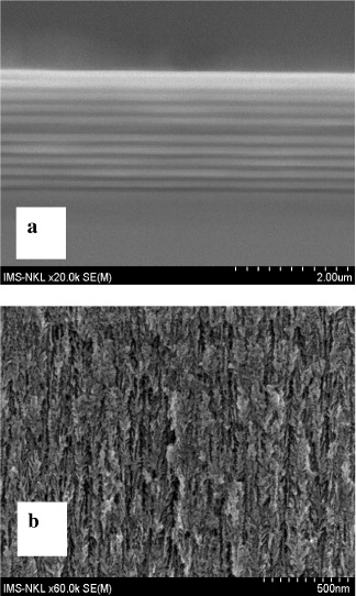
Figure 5 FE-SEM images of microcavity cross section with a λ/2-wavelength thickness spacer for a centered wavelength of 650 nm (a) and a porous silicon size of some tens of nanometers in the spacer layer (b).
Figure 6 shows the experimental reflectivity spectra of the 1D Fabry-Perot microcavity for an incident angle of 8° measured by a UV–VIS–NIR spectrophotometer (Varian Cary-5000). The spectrum is characterized by a transmission resonance at 643.27 nm between two high reflectivity bands. The reflective distinction ratio of 40% and the band-pass FWHM width of 20 nm were observed in a 1D photonic microcavity based on 20 stacked layers of PS.
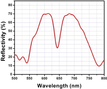
Figure 6 Reflectance spectra of a 12 stacked layer PS microcavity. The linewidth of the pass-band is 20 nm.
The preparation of PS structures composed of several layers of DBR-cavity with a narrow band-width of 2 nm as the design by simulation was difficult, because the line width of reflectance was strongly affected by inhomogeneities in the layers. The anodization condition might drift as the sample thickness and refractive index of stacks, and the solution composition, changes with the depth because of limited exchange through the pores, which caused the difference in experimental results in comparison with the simulation results. In general, the band-width of 20 nm at the visible region obtained from the 1D photonic microcavity based on PS technology is good enable for application in optical sensord, biosensors and/or DBR microcavity lasers. For the prevention of the ageing process of PS layers, we used a thermal annealing process of PS samples to obtain silicon rich silicon oxide (SRSO) materials. The thermal annealing process used for SRSO has four steps: (i) first the PS samples were kept at 60 °C for 60 min in air ambient to stabilize the PS structures; (ii) the pre-oxidation of PS samples was performed at 300 °C for different times varying from 20 to 60 min in oxygen ambient; (iii) slowly increasing the temperature up to 900 °C and keeping samples for 5–10 min in oxygen ambient; (iv) keeping the samples in nitrogen atmosphere at a temperature of 900–1000 °C for 30 min and then the temperature was decreased with very slow rate to room temperature.
Table 2 presents the shift in transmission band in the spectra of a Fabry–Perot microcavity based on the as-prepared and thermally annealed PS layers at 300 °C and 900 °C in oxygen ambient, respectively. The 900 °C oxidation decreases the centered wavelength of transmission by more than 170 nm and the reflective distinction ratio of 15%, while the line width of transmission does not change.
Table 2. Shift of narrow transmission band in the spectra of a 1D porous silicon microcavity after the thermal annealing process (the anodization condition was shown in table 1).
| As-prepared sample | 643.9 | 22.2 | 40 |
| 300 °C/40 min | 565.6 | 22.6 | 34 |
| 300 °C/40 min | 472.5 | 19.2 | 25 |
| +900 °C/5 min |
This can be explained as follows. The centered wavelength of transmission corresponds to the optical thickness of the spacer layer, which is the product of the refractive index and the layer thickness. During the oxidization process at high temperature, the layer thickness and refractive index of the spacer decreased, which caused the shift in transmission wavelength and the decrease in reflective distinction ratio of the microcavity.
5. Conclusion
To conclude, we successfully fabricated a 1D photonic microcavity based on a porous silicon multilayer that has the selectivity of wavelength in a range from 550 to 775 nm, a reflectivity of about 70–80%, and a distinction ratio of 40%. The spectral characteristics of these devices, such as the desired wavelength (λ0), the FWHM line width of band-pass spectrum and the reflectance, were controlled. Simulation programs have been realized for the computational study and design of 1D photonic microcavities. A good correspondence between simulation and experimental results in the transmission wavelengths of the cavity was obtained. The imperfection of interfaces between stacks created by electrochemical etching was used to explain a low distinction ratio and the deformation of the reflective spectrum from a microcavity having few periods. A 1D photonic microcavity in the PS technology has a potential for use in DBR micro-lasers and optical sensors.
Acknowledgments
This work was financially supported by the National Foundation for Science and Technology Development (NAFOSTED) of Vietnam under Grant No. 103.06.38.09. The authors thank Pham Duy Long for supplying the electro-chemical equipment. The apparatus of the National Key Laboratory for Electronic Materials and Devices was used in the experiment.