
Abstract
Cadmium sulfide (CdS) and zinc oxide (ZnO) are used in thin film solar cells as buffer layer and transparent conducting oxide, respectively. The effect of annealing conditions on the morphology and physical properties of CdS and ZnO films prepared using chemical bath deposition and sol–gel synthesis techniques, respectively, was investigated. CdS films obtained from the chemical bath deposition (CBD) process were found to be polycrystalline with dense granular morphology. Electrical characterization of the films annealed at 400 °C for 10 min yielded values of 2.2×10⁻³ Ω cm and 8.3×1012 cm−3 for resistivity and carrier concentration, respectively. Scanning electron microscopy (SEM) and x-ray diffraction (XRD) studies of intrinsic zinc oxide (i-ZnO) films revealed flake-like morphology and transformation of the as-deposited amorphous structure into a hexagonal wurtzite crystal structure upon annealing at 500 °C for 2 h. Optical and electrical characterization results showed that such films had ∼80% transmittance and resistivity values as low as 6.4×10² Ω cm. These films are being explored for fabrication and testing of copper-indium-gallium-(di)selenide (CIGS) thin film solar cells obtained from simple, cost-effective, solution-based synthesis routes.
Export citation and abstract BibTeX RIS

Content from this work may be used under the terms of the Creative Commons Attribution-NonCommercial-ShareAlike 3.0 licence. Any further distribution of this work must maintain attribution to the author(s) and the title of the work, journal citation and DOI.
1. Introduction
Copper chalcopyrites are a class of copper compounds and alloys that assume a tetrahedral crystal structure with various chemical compositions. This class is described by general chemical composition CuIn 1−x Ga x Se 2−y S y , abbreviated as CIGSS, with sulfur sometimes used, in addition to, or replacing selenium [1]. It is a I–III–IV 2 compound semiconductor material whose bandgap value can be tailored from ∼1.0 eV for copper-indium-selenide (CIS) to 1.7 eV for copper–gallium–selenide (CGS). The replacement of In by Ga is also beneficial from a materials availability point-of-view. CIGS-based thin film solar cells have ZnO:Al/ZnO/CdS/CIGS/Mo/SLG multilayer configuration with film thicknesses not exceeding a few microns. Typically, the substrate is soda-lime glass (SLG), polyimide sheet, or stainless steel foil on which a molybdenum (Mo) back contact layer, a p-type CIGS semiconductor absorber layer, cadmium sulfide (CdS) buffer layer, an n-type zinc oxide (ZnO) front contact, and aluminum-doped zinc oxide (ZnO:Al) transparent conductive oxide (TCO) films with certain thicknesses are deposited using a combination of vacuum- and non-vacuum-based synthesis techniques.
The absorber layer can be synthesized via (a) sequential deposition of copper (Cu), gallium (Ga), and indium (In), followed by post-treatment in selenium (Se) and sulfur (S) atmosphere [2], (b) co-evaporation in a one-step process [3], or (c) a three-step method involving sequential evaporation of In/Ga/Se, Cu/Se, and In/Ga/Se at 330–550 °C [4]. The driving forces for CIGS technology are (i) potential high efficiency, (ii) low specific energy for production, and (iii) lowest amount of energy consumed (11 MJ/MW p ) in manufacturing CIGS modules among all technologies [5]. Mass production of CIS/CIGS modules is already in the commercial phase [6–9]. The maximum efficiency of these large-scale modules was measured to be 14.28% [10]. Theoretically, power conversion efficiencies of the solar cells could be increased to a maximum theoretical efficiency, called the Shockley–Queisser limit, of 33.7% [11].
Recent advances in colloidal science and semiconductor nanocrystal synthesis offer immense potential for the development of low cost, and/or high efficiency solar cells. CIGS technology is not, however, without disadvantages, such as a limited supply of indium for mass production [12] and the need to have precise process control for high device efficiency. The indium requirement can be reduced either through reduction in CIGS film thickness from its current optimum value of 1.6–1.2 μm or via replacement of indium with another suitable material such as zinc in the compound, while maintaining the same performance level [13, 14].
CBD CdS and sol–gel intrinsic (i-ZnO) films were prepared and characterized for their composition, structure, surface morphology, optical and electrical properties. The as-deposited films were obtained from spin coating or dip coating of the glass substrates with the precursor solution. The effect of annealing temperature and time on the films was assessed through extensive structural, compositional and physical characterization of the films.
2. Experiment
Microscopy glass slides, sectioned as coupons 10×10 mm in size, were used as substrates. Prior to deposition, the substrates were cleaned in 2 wt.% chromic acid and rinsed thoroughly with distilled water. All the reagents used were of analytical grade purity (>99.99%).
For CdS films, a bath with composition 0.03 M CdCl 2.2.5H 2 O, 0.12 M H 2 NCSNH 2 was prepared whose pH was adjusted and maintained at 10 by means of NH 4 OH buffer solution addition. The substrates were immersed in the bath, kept at 85 °C with continuous stirring, for 30 min. After that, the samples were washed thoroughly using distilled water in order to remove any loosely-adhered CdS precipitates. The films were dried at 180 °C for 15 min in an oven, followed by annealing at 400 °C for different lengths of time.
Sol-gel synthesis of i-ZnO was carried out using zinc acetate dihydrate (ZAD), monoethanol amine (MEA) and iso-propanol (i-PrOH) as precursor salt, stabilizer and organic solvent, respectively. To prepare the sol solution, 0.2 M ZAD was dissolved into i-PrOH followed by the addition of MEA to improve ZAD solubility. The MEA:Zn 2+ ratio was maintained at 0.75. The addition of MEA transformed the initially opaque solution to transparent appearance. Following sol aging for 24 h at room temperature, the substrates were coated with thin film via spin coating at a spin speed of 2000 rpm for 30 s. Immediately after that, the samples were dried at 200 °C for 10 min, thus completing one coating cycle. Three coating cycles were performed for each deposition condition. After that, the films were annealed at 500–600 °C for 2 h, following slow heating (2 °C/min −1) to avoid film microcracking (table 1).
Table 1. Synthesis and annealing conditions for Cds and i-ZnO thin films.
| B1 | 0.03:0.12 | CBD | 85 | 30 | x | x |
| B2 | 0.03: 0.12 | CBD | 85 | 30 | 400 | 10 |
| B3 | 0.03: 0.12 | CBD | 85 | 30 | 400 | 30 |
| i-ZnO window layer | ||||||
| Zn 2+ (Mi), | Process | Spin speed | Time | Temperature | Time | |
| MEA: Zn 2+ | (rpm) | (min) | (°C) | (min) | ||
| iZ1 | 0.2 M, 0.75 | Sol–gel | 2000 | 0.5 | x | x |
| iZ2 | 0.2 M, 0.75 | Sol–gel | 2000 | 0.5 | 500 | 120 |
| iZ3 | 0.2 M, 0.75 | Sol–gel | 2000 | 0.5 | 600 | 120 |
The structural, morphological and compositional characterization of as-deposited and annealed films was carried out using a scanning electron microscope (JEOL, JSM6460) and x-ray diffractometer (STOE, Stadi MP). The optical transmittance and bandgap values were measured from a spectrophotometer (Labomed, UV 2500). The electrical resistivity, carrier concentration and carrier mobility values of the films were determined using a Hall effect measurement system (Ecopia, HMS5000) by making indium ohmic contacts.
3. Results and discussion
3.1. CBD CdS buffer layer
The surface morphology of un-annealed and annealed films was examined under a scanning electron microscope. As shown in figure 1, annealing treatment was found to influence the average surface roughness with a coarse grain structure together with fine pores, obtained for films annealed at 400 °C for 30 min. This observation is somewhat consistent with earlier findings where similar surface morphology together with a higher degree of surface roughness, inhomogeneity and grain growth was reported [15].
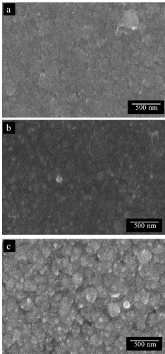
Figure 1 SEM micrographs of CdS film surfaces: (a) no annealing treatment, (b) 400 °C, 10 min, (c) 400 °C, 30 min.
XRD spectra (figure 2) revealed a gradual increase of film crystallinity with longer annealing time, as evident from an increase of relative intensity of the strong peak. The chemical deposition temperature was reasonably high to induce a certain degree of crystallinity into the deposited films. The peaks were indexed to be due to (111), (220), and (311) planes of the cubic structure (JCPDS 80-00019). A small peak located at 25.5° in the case of annealed films is assigned to the (040) plane of the orthorhombic phase. The coexistence of cubic and orthorhombic polymorphs of CdS has also been reported in the literature [16]. Using the Scherer equation, the average crystallite size of the films was estimated and found to increase from 16 nm for un-annealed films to 31 nm for 30 min annealing treatment. Also, the nanocrystalline nature of the CdS films was manifested by a significant degree of peak broadening [17]. From transmittance data as shown in figure 3, the average value of percent transmittance (%T) was up to ∼70% in a wavelength range of 500–900 nm. The crystallite size effect in the nanoscale regime was found to have a significant impact on bandgap values computed from transmittance spectra. The annealing treatment also resulted in better electrical properties, indicating a decrease in resistivity of the CdS films. The best results were obtained for CdS films annealed at 400 °C for 30 min with resistivity and carrier concentration values in the order of 2.2×10³ Ω cm and 8.3×1012 cm −3, respectively.
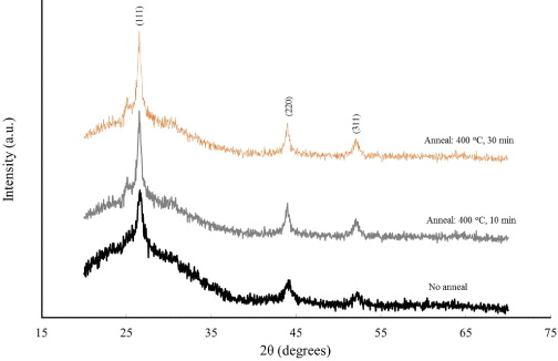
Figure 2 XRD pattern of CdS thin films under different annealing conditions.

Figure 3 Transmittance spectra of CdS thin films with different annealing treatments.
3.2. Sol–gel ZnO window layer
SEM examination of the film surfaces at low magnification revealed granular, irregular flake-like morphology in all cases. Annealing treatment seemed to reduce the degree of surface roughness with relatively smooth films obtained after longer times. It is believed that annealing treatment causes film crystallization and removal of organic residue from as-deposited films. As annealing temperature was increased, uniform and dense, flake-like morphology was noticed. Similar topographical morphology was reported previously for i-ZnO films [18]. Low and high magnification SEM microstructures of film surfaces are presented in figure 4. At still higher annealing temperature, these flakes were observed to have broken down into a fine granular structure. Such morphological change upon annealing at 600 °C is believed to be caused by strain produced in the glass substrate that resulted in stress generation in films which, in turn, led to degradation of film properties. XRD spectra (figure 5) revealed a gradual increase of film crystallinity with annealing treatment, as evident from an increase of relative intensity of the strong peaks. The peaks were indexed to be due to (100), (002), and (101) planes of the hexagonal wurtzite structure (JCPDS 36-1451). The peak intensity for the (002) plane was found to be maximum for films annealed at 500 °C, indicating preferential growth that is characteristic of films having a c axis parallel to the normal of the substrate (c∥n) [19]. The average crystallite size of the films was computed and found to increase from 28 to 58 nm upon increasing the annealing temperature from 500 to 600 °C. The structural degradation of the films annealed at 600 °C observed during SEM examination was also manifested in x-ray diffraction data through deterioration in the degree of crystallization in those films, as evident from reduced peak intensities. Since the value of strain point for glass (550 °C) is less than the annealing temperature (600 °C in this case), the substrate undergoes deformation, thus leading to stresses developed in the films [20].

Figure 4 Low and high magnification SEM microstructures of i-ZnO thin films with different annealing temperatures: (a, b) no anneal, (c, d) 500 °C for 2 h, and (e, f) 600 °C for 2 h.

Figure 5 XRD pattern of i-ZnO thin films with different annealing conditions.
Optical transmittance data (figure 6) indicated that a maximum value of %T in the range of 75–80% was measured for ZnO films annealed at 500 °C for 2 h. The fundamental absorption edge was found to lie near a wavelength of 370 nm. Optical transmittance was noticed to increase in the case of denser morphology due to the reduced degree of light scattering. The transmittance of i-ZnO thin films was expected to vanish near the absorption edge. However, the spectra show some transmittance in the near UV region which may be attributed to poor crystallinity and the presence of nanovoids in the sol–gel-derived ZnO thin films [18]. Electrical characterization of the films indicated strong dependence of electrical properties on the degree of crystallinity in the films. The minimum value of electrical resistivity was determined to be ∼6.4×10² Ω cm obtained for films annealed at 500 °C for 2 h. The corresponding increase of carrier mobility for higher annealing temperatures is primarily due to the combined effect of reduced defect density and relatively large crystallite size. For films annealed at 600 °C, the drop of carrier concentration was because of the reduced degree of crystallinity in the annealed films. For both the CdS buffer layer and i-ZnO TCO films, the main structural, electrical and optical properties derived from characterization are listed in table 2. Beside their intended use as component films for CIGSS-based thin film solar cells, nanostructured ZnO/CdS bilayer films have significant potential as working electrodes in photoelectrochemical cells [21].
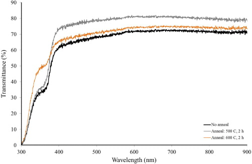
Figure 6 Transmittance spectra of i-ZnO thin films with different annealing conditions.
Table 2. Various properties of as-deposited and annealed CBD CdS and sol–gel i-ZnO films.
| B1 | 16 | – | 2.16×10⁴ | 2.53×10¹⁰ | 65 | 2.49 |
| B2 | 22 | – | 1.60×10⁴ | 1.09×10¹² | 68 | 2.44 |
| B3 | 31 | – | 2.18×10³ | 8.3 ×10¹² | 70 | 2.36 |
| i-ZnO window layer | ||||||
| iZ1 | – | 8.60 | 1.81×10⁵ | 2.12×10¹⁰ | 66 | 3.33 |
| iZ2 | 28 | 7.69 | 6.35×10² | 5.36×10¹³ | 72 | 3.36 |
| iZ3 | 51 | 5.65 | 6.06×10⁴ | 4.56×10¹¹ | 80 | 3.32 |
4. Conclusion
In an attempt to produce CIGSS-based thin film solar cells using solution-based processing routes, CdS and i-ZnO films were prepared using chemical bath deposition and sol–gel synthesis techniques, respectively. The effect of annealing conditions on structural, optical and electrical properties was investigated. In both cases, films were comprised of nanocrystals with strong dependence of average crystallite size on annealing temperature and time.
For CdS films, annealing at 400 °C for 30 min produced films with reasonably low electrical resistivity and up to 70% transmittance. The films had an average thickness value of ∼70 nm. It is highly desirable that the percent transmittance value of such films should be increased beyond 85% for better cell performance. This can be accomplished through further process optimization and taking into consideration other process parameters such as bath chemistry, deposition temperature, etc.
Intrinsic ZnO films with excellent optical and electrical properties were obtained after annealing at 500 °C for 2 h. Yet again, the %T values need to be enhanced for the effective use of such films in thin film PV technology. Work is in progress to obtain films with the same, if not better, attributes than those of vacuum-deposited films.
Acknowledgments
This research effort was jointly sponsored by the Higher Education Commission, Pakistan through grant no. 20-1603 and the National University of Sciences and Technology (NUST), Islamabad.