
Abstract
Micrometer-long titanium oxide nanotube arrays, tens of nanometers in diameter, were fabricated by anodization of titanium film coated on a conducting glass substrate. The Ti film was deposited by magnetron sputtering at room temperature. The effect of anodizing conditions on the formation of TiO2 nanotubes was investigated. The results indicate that dense and uniform Ti film deposited under 150 W at room temperature was favorable for the formation of ordered nanotube arrays. The average diameter of the TiO2 nanotubes varied from 35 to 95 nm when the anodization potential changed from 10 to 40 V. Micrometer-long nanotubes (1.1 μm) with good adhesion to the substrate could be obtained in 0.5 wt% NH4F/glycerol at 30 V for 2 h. After heat treatment, the crystalline anatase nanotubes show enhanced photoelectrochemical activity compared with those anodized in 1 M H3PO4/0.5 wt% HF. This is attributed to the increased light-harvesting abilities.
Export citation and abstract BibTeX RIS

Content from this work may be used under the terms of the Creative Commons Attribution-NonCommercial-ShareAlike 3.0 licence. Any further distribution of this work must maintain attribution to the author(s) and the title of the work, journal citation and DOI.
1. Introduction
Since Zwilling et al demonstrated the possibility of growing self-organized and ordered TiO 2 nanotubes by anodic oxidation of titanium and its alloys [1], there have been many attempts to improve the structure and to exploit the functionality of these highly organized structures [2, 3]. In view of exploiting specific TiO 2 properties, a good deal of attention has been given to applications in photovoltaic cells [4], photocatalysis [5], sensing [6] and wettability-based templates [7] due to the unique physical and chemical properties. Many approaches such as templated synthesis, hydrothermal reaction and anodic oxidization have been developed for the preparation of TiO 2 nanotubes. Among them, anodic oxidization is a relatively simple technique that can be easily automated for preparing highly oriented and uniform nanotube arrays [2, 8]. However, most work has focused on the anodization of titanium foils, which limits application in functional microdevices [9, 10] as the titanium metal underneath the nanotubes may result in an electrical short-circuit. Another problem with Ti foil-based devices is their susceptibility to mechanical shock/vibrations; the high stress created at the ceramic–metal interface may cause device failure. Furthermore, the opaque metal Ti limits the application for some optical-electric devices (e.g. dye-sensitized solar cells or electrochromic devices) in which a transparent metal oxide electrode is required. Therefore, it is imperative to develop methods for the fabrication of highly ordered titania nanotube arrays from Ti thin films on any substrate.
It is of great technological interest to form such nanotube/nanoporous layers from titanium thin films. Recently, some groups have successfully developed the technology to grow nanotube arrays from titanium thin films using anodization on a variety of substrates including glass [9, 11–13], conducting glass [4, 14–22] and silicon [10, 23–25]. Although the electrochemical surface process is the same as for bulk titanium foils, titanium films may be rapidly etched away in acidic HF or neutral fluoride-containing solutions (forming soluble [TiF 6]2- complexes) because the chemical dissolution rate is considerably high [23] and the quality (density, uniformity) of the titanium film and the anodization parameters are critical to the formation process of titania nanotubes [9, 15]. Moreover, the electrolyte was kept at low temperatures in order to decrease the chemical dissolution rate of the oxide layer formed in acidic solution. So far, different types of fluoride-ion-containing electrolytes have been applied to fabricate thin films of TiO 2 nanotubes with different lengths. A 360 nm thick transparent nanotube layer was obtained using solution containing 0.5% (vol) HF and acetic acid [4, 9, 15]. Yu et al [10, 24] and Leenheer et al [16] fabricated the nanoporous TiO 2 layer on silicon and glass substrate with length from ∼100 to ∼500 nm using different types of fluoride-containing solutions. Nanotube lengths ranging from 380 to 700 nm were demonstrated by anodization in H 3 PO 4/HF [26], HF/H 2 SO 4 [23], H 3 PO 4/NaOH/HF [27], Na 2 SO 4/C 6 H 8 O 7·H 2 O/NaF or glycerol/NH 4 F [25] and ethylene glycol/NH 4 F [19] by controlling the pH and temperature and the electrolyte concentrations. However, the length of the nanotube arrays was limited because of the limitations imposed by the quality and thickness of the Ti films [4, 9, 10]. For photoelectrochemical applications, optimized nanotube layers for practical applications strongly depend on their geometrical factors, such as the diameter, wall thickness and tube length. Among them the tube length is important for carrier transport within the tube walls [28]. A longer tube length should enhance the light absorption and thus increase the light-utilization efficiency.
Very recently, micrometer-long TiO 2 nanotubes have been successfully obtained by different groups by anodization of Ti film in NH 4 F/ethylene glycol/H 2 O [18, 21, 22]. According to their work, the substrate needs to be heated to high temperatures (>300 °C) [18, 21, 22] to form a dense, uniform titanium film suitable for anodization. However, this high temperature thin film deposition poses some limitations in certain practical applications, e.g. it is not appropriate to deposit Ti film at high temperature on flexible but low glass transition polymer substrates. Therefore, it is desirable to deposit high quality Ti film with good adhesion at room temperature. In this work, a well-oriented and uniform TiO 2 nanotube layer more than 1 μm long has been fabricated on conducting glass substrate by anodization of titanium film deposited at room temperature. With the success of achieving high quality titanium film at low deposition temperature and subsequent anodization to produce ordered titania nanotube arrays, this new technique makes it possible to produce photovoltaic and sensing devices on flexible organic substrate. Moreover, in order to increase the thickness-conversion ratio from Ti film to TiO 2 nanotube, an electrolyte (NH4F/glycerol) with low chemical dissolution rate was selected.
2. Experiment
2.1. Deposition of titanium film on conducting glass
Ti films (1.5–2.0 μm) were deposited by radio frequency (RF) magnetic sputtering on fluorine-doped tin oxide-coated conducting glass (FTO). A target of 99.9% Ti was used. The base chamber pressure was below 7.0×10⁻⁴ Pa. Deposition was carried out under an Ar flow rate of 10 sccm, and the distance between the target and sample was 60 mm. During the deposition process, the argon gas pressure was 0.5 Pa and the applied sputtering power was 70–80 W and 150–165 W. To remove pinhole defects in the titanium film, the specimen was sequentially cleaned in an ultrasonic bath of acetone, ethanol and deionized water for 10 min each.
2.2. Preparation of TiO2 nanotubes on FTO glass by anodization
Anodization was carried out using a two-electrode configuration. The experimental setup is shown in figure 1. The FTO substrate with an exposed titanium film surface area of 1.0 cm 2 was fixed to a titanium foil. It was then attached to a copper rod to form the working electrode. The titanium foil was protected by a non-conductive epoxy in order to avoid being anodized in the electrolyte. A platinum sheet (2.0×1.5 cm 2) connected to a copper wire was used as the counter-electrode. The distance between the working and counter-electrodes was kept at 3.0 cm. A dc power source (model WYK-1502) supplied the required anodization potential in a single step (without ramping). Anodization was conducted in 0.5 wt% NH 4 F/glycerol and 1.0 M H 3 PO 4/0.5 wt% HF (for comparison) at room temperature. After anodization, samples were immediately washed in distilled water and subsequently dried in air. The samples were heat treated at 450 °C in air at a heating rate of 5 °C min −1, and then the samples were cooled in a furnace, generating the anatase phase of TiO2 nanotubes.
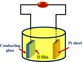
Figure 1 Experimental setup for the anodization of Ti thin film on conducting glass.
2.3. Characterization
The phase composition of the sample was identified by x-ray diffraction (XRD) using a Shimadzu 6000 x-ray diffractometer with Cu K α radiation (λ=1.541 78 Å). The morphologies were examined using a field emission scanning electron microscope (FESEM; LEO-1530VP). All photoelectrochemical measurements were carried out in electrolyte solution of 0.1 mol l −1 Na 2 SO 4 under ultraviolet lamp (UV, 254 nm, 8 W) illumination using a three-electrode system.
3. Results and discussion
The quality of the titanium film is critical to the formation of TiO2 nanotubes. The effect of deposition parameters on the structure of sputtered Ti films and TiO 2 nanotubes was systematically studied in our previous work [12, 26]. It was found that with the increase of sputtering pressure, the deposition rate of Ti films increases but the density decreases. Additionally, increasing the substrate temperature or sputtering power could improve the density and the crystallinity of the films.
In this work, the thin film was deposited at ambient temperature without any heating with a working Ar pressure of 0.5 Pa. It is found that at low sputtering powder (75 W), the size of the nano-grains in the Ti thin film was non-uniform and the surface roughness was high (figures 2(a) and (b)). The thin film could be easily peeled off from the substrate during anodization. With increasing sputtering power, the Ti atom obtains higher energy and its surface diffusion is improved. It was observed that a smooth Ti film composed of hexagonal nano-grains with sizes of 100–200 nm (figure 2(c)) was obtained at 150 W. The columnar structure with high density is clearly seen from the cross-section of the film (figure 2(d)). From the XRD pattern (figure 2(e)), it was found that the Ti film obtained at low sputtering power exhibits no preferred orientation. It shows clear preferred orientation along the (002) plane when the film is deposited at high power of 150 W. Moreover, the crystallinity of Ti films is significantly increased and the thin film has good adhesion with the substrate. We found that this deposition condition is suitable for the following anodization experiment.
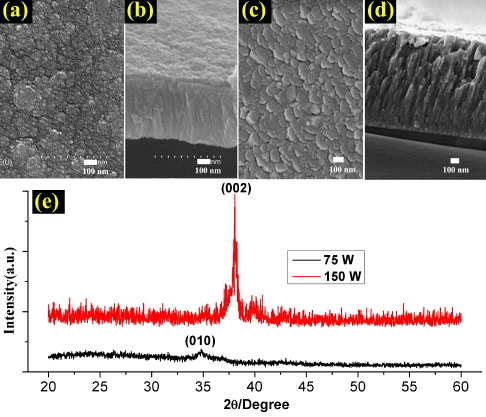
Figure 2 FESEM images and XRD patterns of Ti films deposited on glass substrates under sputtering power of (a, b, e) 75 W and (c, d, e) 150 W at ambient temperature.
Figure 3 shows polarization curves (a) from 0 to 10 V with a sweep rate of 50 mV s -1 and subsequent current–time behavior (b) recorded at 10 V in 1.0 M H 3 PO 4+0.5 wt% HF and 0.5 wt% NH 4 F/glycerol. Clearly, active passive transition occurs at the beginning of the experiment, and then a second current increase occurs at about 3300 mV in the H 3 PO 4/HF electrolyte (figure 3(a)). Such behavior is frequently observed in the aqueous fluoride-containing electrolyte for anodic pore-forming reactions that display self-organization [29]. However, this phenomenon is not obvious in the NH 4 F/glycerol electrolyte due to its high dielectric constants and viscosity. A low current density was found in the viscous electrolyte, which is one-tenth of the H 3 PO 4/HF electrolyte. This indicates that the anodization process is controlled by diffusion and hence the dependence of the diffusion constant on the viscosity in a Stokes–Einstein manner: D=k B T/6πηr, where k B is Boltzmann's constant, T is the absolute temperature, η is the dynamic viscosity and r is the radius of a spherical body. Therefore, a lower current density with weaker local acidification and lower chemical dissolution rate of the nanotube can be obtained for viscous electrolytes. During the initial anodization process the current rises and then drops to a minimum because of the formation of compact oxide film. After an initial decrease, the current increases slowly for a short time as the titania nanotube layer starts to form. Then the current starts to decay again as the titanian nanotubes become thicker and more resistive while the titanium film below the oxide layer becomes thinner. The result is consistent with earlier work [3, 29]. As the last of the Ti film is consumed, the current suddenly increases because the electrolyte, especially for aqueous solution (figure 3(b)(B)), is interacting with the FTO surface. At this point, the sample must be quickly removed from the electrolyte to preserve the nanotubes or else it will be consumed by the HF. Moreover, the curve of glycerol electrolytes is smooth and no fluctuation is observed (figure 3(b)(A)), and this phenomenon also occurred at high voltage (20–40 V), which means that the deposited Ti film was favorable for the formation of ordered nanotube arrays. However, occasional fluctuations in current were found during the anodization process for the H 3 PO 4/HF electrolyte. Due to the high potential and low viscosity of the aqueous fluoride-containing electrolyte, oxygen bubbles (2H 2 O-4e → 4H ++O 2↑) were observed on the pinholes in Ti film or any exposed FTO substrate. The formation of O2 will cause current fluctuations, but it did not appear in the glycerol electrolyte.
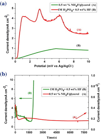
Figure 3 Polarization curves (a) and current versus time characteristics (b) of samples anodized in the following electrolytes: 0.5 wt% NH 4 F/glycerol and 1.0 M H 3 PO 4/0.5 wt% HF at 10 V.
Figure 4 shows FESEM images of samples anodized in 0.5 wt% NH 4 F/glycerol with potentials ranging from 10 to 40 V at room temperature. Obviously, the potential has a significant impact on the tube diameters and the tube diameters increase almost linearly with the increase of anode potential (figure 5).
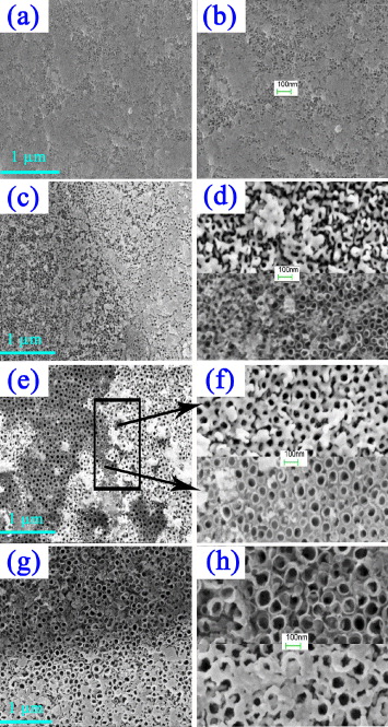
Figure 4 FESEM images of the TiO 2 nanotube layers formed at different conditions. (a, b) (c, d) (e, f) and (g, h) are images of Ti films anodized at 10, 20, 30 and 40 V for 2 h, respectively. (d, f and h) Each show two locations selected from (c, e and g).
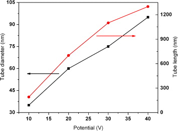
Figure 5 The relationship of length (squares) and diameter (circles) of the TiO 2 nanotube versus anode potential. The anodization was conducted in 0.5 wt% NH4F/glycerol at room temperature for 2 h.
It is noticed that there was a largely uniform oxide layer on top of the nanotube structure, and this layer was not completely removed, even after 2 h anodization (figures 4(a), (c), (e) and (g)). Higher anodizing potential seems to be able to remove more of this layer. This indicates that higher potential not only increases the electric field intensity of the oxide layer but also speeds up the diffusion of ions, leading to acceleration of the field-enhanced dissolution of this porous oxide layer. Figures 4(b), (d), (f) and (h) are high magnification of figures 4(a), (c), (e) and (g), respectively. The surface of as-fabricated nanotubes shown in figure 4(e) (enlarged in figure 4(f)) was composed of the top oxide layer and arrays of nanotubes. This phenomenon accounts for the progression in layer morphology from a thin and compact titania oxide formed at the beginning to a porous structure, under which nanotubes are formed. A clear TiO 2 nanotubular structure appears when most of the top oxide layer was chemically dissolved in the anodization. As the chemical etching rate of viscous electrolytes is low, a considerable length of time is required to fully dissolve the top titania oxide layer. The nanotube length–voltage curve in figure 5 indicates that a faster growth rate is obtained at higher anode potentials. After 2 h anodization, the nanotube length reaches around 190, 700, 1100 nm, and 1300 nm at anode potentials of 10, 20, 30 and 40 V, respectively. However, it is found that the nanotubes became fragile and would detach from the substrate if the reaction time reaches 3 h when the applied potential rose to 40 V, which is due to the over-anodization of the thin Ti film since it had been transformed into the TiO 2 nanotube. Thus, suitable anodization parameters must be carefully chosen during the processing of titania nanotubes on FTO glass.
It has been found that chemical etching can efficiently remove the porous oxide layer on the TiO 2 nanotubes [4, 14]. In order to completely remove the top oxide layer on the surface, as-prepared samples were cleaned by chemical etching in 0.05 wt% HF solution with the aid of ultrasonic treatment. Comparison was made with the same chemical etching without ultrasonic treatment. Figure 6 shows the surface topography of the samples after chemical etching treatment for 30 s. It is found that some part of the cover layer on the TiO 2 nanotube surface was dissolved and peeled off from the nanotubes after 15 s (not shown), and uniform nanotube arrays were formed after 30 s treatment (figures 6(a) and (b)). The cross-sectional image in the inset of figure 6(b) shows that the nanotubes are very smooth with a tube length of about 1100 nm (figure 5). Without the ultrasonic action, the removal of the oxide layer was much less effective, as evidenced by figure 7. There was no significant change of the thin film morphology after 15 s (figure 7(a)), and some of the oxide layer still remained after immersing for 30 s (figure 7(b)). Compared with chemical etching alone, ultrasonic-chemical cleaning was found to be able to remove the top oxide film from the nanotube surface much more easily. Therefore, ultrasonic-chemical cleaning is a very efficient method for removal of the top oxide layer.
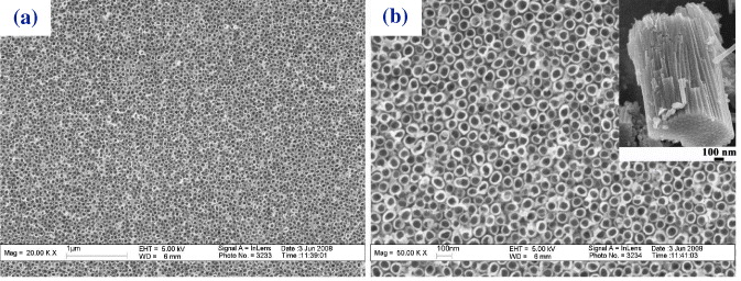
Figure 6 FESEM images with (a) low and (b) high magnification of the TiO 2 nanotube layers obtained after chemical etching in 0.05 wt% HF solution with the aid of ultrasonic treatment for 30 s. The inset in (b) is a cross-section of the nanotubes. The as-prepared TiO 2 nanotube samples before treatment are formed 30 V for 2 h in 0.5 wt% NH 4 F/glycerol.
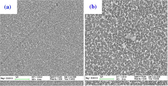
Figure 7 FESEM images of the as-prepared nanotube surface immersed in 0.05 wt% HF for (a) 15 s and (b) 30 s without ultrasonic treatment. The as-prepared TiO 2 nanotube samples before treatment are formed 30 V for 2 h in 0.5 wt% NH 4 F/glycerol.
Comparison was made of photocurrent generation under UV illumination between nanotubes of different lengths fabricated in 0.5 wt% NH4F/glycerol and 1.0 M H 3 PO 4/0.5 wt% HF in a home-made photoelectrochemical testing setup (figure 8(a)). Since the as-prepared nanotubes had amorphous phase, the samples were heated at 450 °C in air for 3 h to obtain the crystalline anatase phase following a well-adopted practice [26]. The measurements were carried out in an electrolyte solution of 0.1 mol l -1 Na 2 SO 4 under ultraviolet lamp (UV, 254 nm, 8.0 W) illumination by using a three-electrode system at room temperature with the TiO2/FTO electrode, a platinum plate and a saturated calomel electrode (SCE) serving as the working, counter and reference electrodes, respectively. The distance between the working electrode and the UV lamp was 30 mm. As shown in figure 8(b), the photoelectrochemical current transiently increased and then stabilized when UV light was turned on at 50–100 s, which indicates that the nanotube electrode has good photoelectric current stability. However, once the UV light was turned off (at 100 s), the photocurrent intensity quickly decreased to the initial dark current. This phenomenon illustrates that composite electrodes have n-type semiconductor characteristics. The photocurrent of the sample with longer tubes was constant at 1.55 μA under dark conditions and then drastically increased to 9.78 μA under UV illumination. It shows better performance than the 380 nm-long transparent nanotubes as reported previously [26]. The better performance is due to a longer tube length that gives rise to a large illumination area, and the photo-generated electron can be efficiently separated and travel to the conducting glass before recombination.
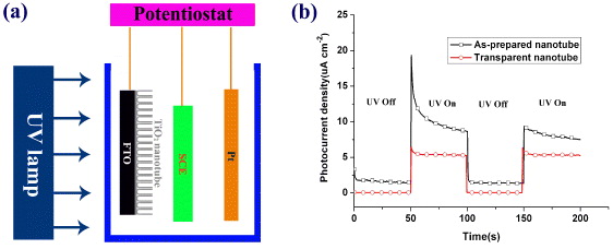
Figure 8 (a) Schematic illustration of the photoelectrochemical testing setup; (b) comparison of the photocurrent response between nanotubes of different lengths in 0.1 mol l −1 Na 2 SO 4 solution under UV pulsed-illumination. The tube length of the as-prepared nanotube and transparent nanotube is 1.1 and 0.38 μm, respectively.
4. Conclusion
Micrometer-long TiO 2 nanotube arrays were successfully formed on FTO glass by anodization of sputtered titanium film. The results show that the dense, crystalline and uniform Ti film obtained by room temperature sputtering was suitable for the formation of ordered nanotube arrays. Using highly- viscous 0.5 wt% NH4F/glycerol solution enables the successful formation of such micrometer-long tubes with improved photocurrent performance. Compared with the shorter TiO 2 nanotube formed in 1.0 M H 3 PO 4/0.5 wt% HF, the as-prepared longer tube length enhances the light absorption and thus increases the light-utilization efficiency.