
Abstract
Ultraviolet (UV) photoluminescence (PL) data taken on a double Au implanted Si matrix are reported. This has been studied over a wide temperature range of 28–220 K. At low temperature, the spectrum shows four peaks corresponding to a zero-phonon line (ZPL) and three low-energy phonon-assisted lines. At 28 K the ZPL has an energy of 3.362 eV with a lifetime of ∼240 ps suggesting transitions across a direct gap. The temperature variation of the ZPL intensity indicates an activation energy ∼10 meV comparable to the binding energy of excitons in crystalline Si (c-Si). For T > 100 K, it shows a redshift which can be understood as coming from exciton–phonon interaction. At lower temperatures the corresponding line broadening shows evidence of interaction with low-energy phonons of average energy ∼7 meV as suggested earlier. All the above results indicate the emission to be coming from Si nanoclusters (NCs) embedded in the matrix.
Export citation and abstract BibTeX RIS

Content from this work may be used under the terms of the Creative Commons Attribution-NonCommercial-ShareAlike 3.0 licence. Any further distribution of this work must maintain attribution to the author(s) and the title of the work, journal citation and DOI.
1. Introduction
Crystalline Si (c-Si) being an inefficient light emitter is an impractical material for photonic applications. The indirect radiative interband transitions in bulk c-Si are strongly suppressed because an emitted photon cannot satisfy momentum conservation for transition from the bottom of the conduction band to the top of the valence band. The only way to have a radiative indirect transition without violating momentum conservation is via the emission of a phonon. This also has a small probability due to weak electron–phonon interaction. This leads to a substantial increase in recombination time and decrease of recombination probability as compared to no-phonon transitions in direct band gap semiconductors. As shown by Canham in porous Si (p-Si) [1], this can be avoided in nanoscale where visible luminescence has been observed. In such a case, zero-phonon optical transitions are partially allowed with the corresponding oscillator strengths significantly enhanced [2]. Following the initial work on p-Si, a lot of studies have been conducted in Si nanoclusters (NCs) [3, 4] and PL has been observed in wavelengths ranging from UV to the near-infrared [5–8].
But the origin of PL emission from Si NCs is still under debate. The presence of defects and contaminations on the surface results in lower energy emission, which does not go well with quantum confinement [6, 9]. They result in lifetimes in the range of several μs, unlike the emission from the NC core which has a much shorter lifetime [10, 11]. Although most reports indicate emissions from quasi-direct transitions in the visible wavelengths, there are also reports on higher energy emission in the blue or UV range [5, 12–15]. Based on an interband transition model, sharp UV emission from NaF prepared p-Si has been explained as coming from the direct-gap E1 transition [5]. Some earlier data on low-temperature blueshift in the fast UV PL of Si NCs, embedded in amorphous Si (a-Si), also suggest direct band gap emission [13]. In contrast, supported by infrared absorption data, fast PL emission from p-Si in blue and UV have been correlated with oxygen induced surface effects [14,16]. Very recently, direct gap-like UV emission has been reported from pulsed laser deposited alumina capped Si NCs [17]. Although oxygen induced effects have not been ruled out the data suggest direct bandgap emission. Here we report similar UV emission from Si NCs formed in an Au implanted Si matrix. At low temperatures we find emission from a sharp zero-phonon- like transition corresponding to a direct gap. This zero-phonon line (ZPL) has a single exponential decay with a sub-ns lifetime. In addition to the ZPL we see some phonon mediated transitions even at temperatures higher than 100 K, not seen earlier. The ZPL intensity coming from the implanted matrix shows an activation energy close to the binding energy of excitons in c-Si. These observations indicate the emission to be coming from crystalline Si NCs formed in the implanted matrix. Si NCs have earlier been synthesized in SiO 2 using Si implantation [18–21]. In such cases PL emission has been observed in the visible and UV wavelengths. But the spectra are found to be too broad even at low temperatures [18]. Further, the decay lifetimes have been found to be stretched exponentials indicating exciton transport between NCs. Unlike that in the present case, the observed ZPL has a narrow width ∼25 meV. It has a single exponential lifetime ruling out any exciton transport between NCs.
2. Experiment
A 32 keV Au implantation to a fluence of 5×10¹⁵ atoms cm −2 was used to amorphize a 30 nm top layer of a Si substrate (n-type, P doped 1–20 Ωcm). A second 3 MeV Au irradiation to a fluence of 5×10¹⁵ atoms cm −2 has been used to create Si NCs in the top amorphous layer. The sample was further annealed in air at 800 K for 1 h. Electron microscopic images showed the presence of Si NCs of average size 2.15 nm. Steady state PL (SSPL) measurements have been carried out on the sample at temperatures ranging from 28 to 220 K, at an excitation wavelength of 325 nm using a He–Cd laser together with a Jobin-Yvon TRIAX-320 spectrometer. The decay characteristics in different emission regions have also been studied with time resolved PL (TRPL) measurements carried out using a mode locked, frequency doubled, Ti:sapphire laser (350 nm, pulse width 80 fs, repetition rate 80 MHz) together with a Hamamatsu C4334 streak camera system.
3. Results and discussion
The SSPL spectra recorded at 325 nm, for various temperatures between 28 and 220 K, are shown in figure 1. At the lowest temperature 28 K we see a sharp peak at 3.362 eV with a width ∼25 meV which is clearly seen in figure 2. This is associated with three satellite peaks (figure 1). As shown in p-Si, at room temperature [5], electron hole recombinations, coming from quasi-direct transitions, result in broader line-shapes with peaks between 2 and 2.7 eV. The spectrum also shows a sharp peak around 3.3 eV which has been argued as coming from E1 transition across the direct gap at L-point. This has been pointed out to be a characteristic feature of 0-D Si in p-Si samples [5]. At lower temperatures the corresponding gap is ∼3.37 eV. In view of this we take the 3.362 eV line as the ZPL coming from the above mentioned E1 transition. This ZPL is seen to have a symmetric shape suggesting emission from bound-excitons. It further shows a single exponential decay (inset of figure 2) with a lifetime of 240 ps. Such a fast decay is consistent with the high value of confinement energy EC (∼2.2 eV) where an exponential growth in radiative recombination rate is expected [11]. With this identification, the peak at 3.308 eV with a separation of 54 meV, closely matching a TO or LO phonon energy (58 or 53 meV) in c-Si [22], corresponds to the one-phonon line. The next peak is seen to lie about 126 meV below the ZPL. This closely agrees with the two-phonon energy of 122 meV in Si as seen in both absorption and emission data [23, 24]. The third satellite near 200 meV below the ZPL corresponds to higher order phonon involvement. With increase in temperature, the ZPL (figure 1) is seen to show no shift up to about 100 K beyond which there is a red shift. The observed red shift of the ZPL can be understood as due to exciton–phonon interactions. At room temperature all structures merge to a single peak of width ∼100 meV near 3.3 eV as seen earlier [5, 12]. This is quite different from the case of alumina capped Si NCs where the PL signal is seen to vanish above 70 K [17]. In semiconductors the variation of band gap with temperature, T, is usually described using the Varshni equation [25] as given by

Here α describes the fall at higher T, β corresponding to some phonon temperature of the order of Debye temperature. The above equation has been used here to explain the red shift observed at T > 100 K. For such an analysis we have unfolded the ZPL and the one-phonon peaks using Lorentzian structures. The ZPL peak energy, E(T), with temperature T, as obtained after the unfolding, is shown in figure 3. One can see, below 100 K there is no shift in the ZPL. This is unlike an earlier report where low-energy PL emission was seen to have a sharp blueshift with drop in temperature below 50 K [26]. This blueshift has been argued as coming due to exciton migration from larger to smaller NCs [27]. Hopping and migration of excitons is also known to result in a stretched exponential decay of the ZPL [28]. In our case, assuming no exciton migration, the energy given to the NC system appears to result in a broadening of the line-shape with no lowering of energy. This also explains why we see a single exponential decay. Our results are also unlike the data on alumina capped NCs where below 100 K a redshift has been observed in PL with rise in temperature [17].
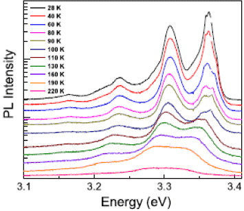
Figure 1 SSPL spectra of Si NCs recorded at different temperatures. Spectra are vertically shifted for clarity.
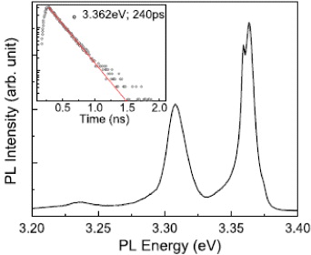
Figure 2 SSPL spectrum recorded at 28 K together with the decay curve for the ZPL (3.362 eV) shown in the inset.
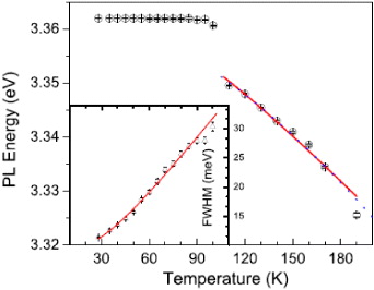
Figure 3 Energy of the ZPL as a function of temperature. The dashed and the solid lines show fits to the experimental data using equations (
For c-Si, α and β are known to have values 7.02×10⁻⁴ eV K −1 and 1108 K, respectively [25]. In the present case, for the region above 100 K, we could get a good fit with experimental data with a β value of 673 K. The results indicate E(0) to be 3.363±0.001 eV as expected and an α value of (8.2±0.4)×10−4 eV K −1 which is quite comparable to that for c-Si. This fit is shown in figure 3 for comparison. The variation of the ZPL energy with T, coming from exciton–phonon interaction is often also fitted to an expression [29]

Here A and κ
B
correspond to the exciton–phonon interaction strength and the Boltzmann constant, respectively, ℏ Ω being the average phonon energy. A fit using equation (

where Γ (0) is an inhomogeneous line-width due to exciton–exciton, exciton–carrier interactions.
Scattering by defects and impurities also contributes to this. Γ
ep
represents an average exciton–phonon coupling strength, ℏ Ω being the average phonon energy. We have used this to understand the low-temperature behavior of ZPL which was not possible for the redshift data. The low-temperature variation of the ZPL line-width (FWHM) with T is shown in the inset in figure 3. A fit to the data using equation (
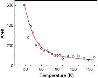
Figure 4 Variation of the ZPL area with temperature. The solid line shows the best fit to the experimental data which indicates an exciton binding energy ∼10 meV.
Most importantly, the UV excitation used in the experiment has a range less than 10 nm in Si (amorphous or crystalline) while the oxide layer on the surface (expected to be about ∼8 nm after annealing) is a transparent one. So the observed signal is primarily from the top 10 nm of the implanted region and not from the bulk c-Si lying underneath. Emission with an exciton binding energy of about 10 meV from this layer indicates the presence of Si NCs in the amorphized matrix. The momentum or the energy conserving (as expected for NCs) phonon replica also indicate crystalline structure ruling out emission from the random oxide layer. Since the NCs are produced below the surface, no oxygen-induced surface effects are expected as seen in p-Si or NCs embedded in SiO 2. It must also be added here that in the present case we have seen PL emission at considerably higher temperatures, unlike in other experiments. As reported earlier this is mainly due to the presence of Au nanoparticles in the medium which results in enhancement of PL signal from surface plasmon excitations [12].
4. Conclusion
To conclude, we have carried out a systematic study of temperature dependence of PL emission from Si NCs synthesized in Si through a two-stage Au implantation. At low temperature the emission is seen to consist of fast, direct and few-phonon-assisted lower energy transitions. The zero-phonon line with a sub-ns lifetime and small activation energy of 10 meV is seen to correspond to excitonic recombination in Si across a direct gap. The single exponential decay of the ZPL indicates the emission to be coming from confined excitons with no migration between NCs.