
Abstract
This paper describes a glucose electrochemical biosensor, layer-by-layer fabricated from graphene and polyaniline films. Graphene sheets (0.5×0.5 cm2) with the thickness of 5 nm (15 layers) were synthesized by thermal chemical vapor deposition (CVD) under ambient pressure on copper tapes. Then they were transferred into integrated Fe3O4-doped polyaniline (PANi) based microelectrodes. The properties of the nanocomposite films were thoroughly characterized by scanning electron microscopy (SEM), Raman spectroscopy, atomic force microscopy (AFM) and electrochemical methods, such as square wave voltametry (SWV) and chronoamperometry. The above graphene patterned sensor (denoted as Graphene/Fe3O4/PANi/GOx) shows much improved glucose sensitivity (as high as 47 μA mM−1 cm−2) compared to a non-graphene one (10–30 μA mM−1 cm−2, as previously reported in the literature). It can be expected that this proof-of-concept biosensor could be extended for other highly sensitive biodetection.
Export citation and abstract BibTeX RIS

Content from this work may be used under the terms of the Creative Commons Attribution-NonCommercial-ShareAlike 3.0 licence. Any further distribution of this work must maintain attribution to the author(s) and the title of the work, journal citation and DOI.
1. Introduction
Although the glucose sensor was developed by Clark and Lyons in 1962, it continues to become more and more important thanks to its applications in biological, chemical analyses, clinical detection and environmental monitoring [1, 2]. The immobilization of enzymes on electrodes is generally the first step in fabrication and has attracted significant efforts, because enzymes are highly selective and quickly responsive to specific substrates [3, 4]. Nanomaterials (such as graphene, carbon nanotubes (CNTs), gold nanoparticles, metal oxides and semiconductor nanostructures) are advantageous for immobilizing enzymes as they maintain enzyme bioactivity due to their microenvironment. These materials can also increase the direct electron transfer between the enzymatic active sites and the electrode [5, 6]. Among the above-mentioned materials, graphene is a two-dimensional plane sheet with open structure (unlike CNTs with rolled structured and metal nanoparticles with different sizes and shapes), hence both sides of graphene could be utilized for enzyme immobilization. Through strong π–π stacking and van der Waals interaction between layers, however, graphene is easily agglomerated or even stacked to form graphite. To solve this limitation, some authors have suggested attaching other molecules or polymers onto the graphene surfaces [7–10].
In this work we propose to transfer graphene films (synthesized by the CVD method) to the layer-by-layer Fe 3 O 4/PANi pre-formed interdigitated array (IDA). The schematic representation of graphene patterning on IDA was shown in figure 1. The advantages of graphene patterned layer-by-layer fabricated electrode, such as excellent analytical quantification of glucose with wide linear range, good sensitivity, good reproducibility and long-term stability, are clearly demonstrated. Furthermore, this promising electrode platform could be extended for the development of other electrochemical biosensors and biomedical devices.
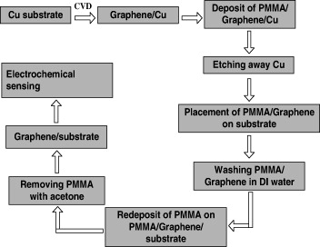
Figure 1 Schematic representation of graphene patterning on IDA for glucose detection.
2. Experimental
2.1. Graphene film synthesis by CVD method
A schema of the CVD setup used for graphene film synthesis is shown in figure 2. A 1.2 m long (22 mm ID) quartz tube is horizontally placed inside a hot wall tube furnace (designed locally and capable of reaching 1100 °C) and served as the CVD system. The horizontal tube furnace allowed rapid cooling, simply by opening it. In addition, samples were also cooled rapidly by shifting the oven out of position of the samples through a system of rails.
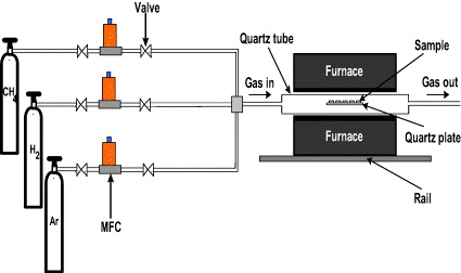
Figure 2 Schematic drawing of the assembled CVD setup used for the synthesis of graphene films.
The substrates for graphene growth were smooth copper (Cu) tapes with a thickness of 70 μm and a size of 0.5 cm ×0.5 cm. The samples were loaded into a quartz tube and then furnace temperature was raised to growth temperature 900 °C in argon (Ar) environment (1000 sccm). To reduce the native copper oxide on the Cu tape surface the samples were kept at CVD temperature for 20 min in a flow of Ar and hydrogen (H 2, 15 sccm). After 20 min a flow of methane (CH 4, 30 sccm) was introduced for growth time of 5 min. After the CVD reaction, the samples in the quartz tube were cooled down to room temperature at the rate about 10 °C min −1 under a flow of Ar (1000 sccm). The graphene films on Cu tapes were then characterized by scanning electron microscopy (SEM), Raman spectroscopy and atomic force microscopy (AFM) techniques.
2.2. Fabrication of graphene/Fe3 O4/PANi/GOx IDA for glucose detection
Fe 3 O 4 nanoparticles (NPs) were synthesized by the co-precipitation method of Fe 3+ and Fe 2+ under alkaline condition. 4 ml of ferrous chloride (1 M) and 2 ml of ferric chloride (1 M) were thoroughly mixed, using magnetic stirring, in a three neck flask of pH 4.0 at room temperature. The solution was vigorously stirred under nitrogen atmosphere followed by drop wise addition of an aqueous solution of 2 M NH 3 into the flask until the black precipitate was obtained. The Fe 3 O 4 NPs were collected with the help of a magnetic field separation on the round-bottomed flask. These Fe 3 O 4 NPs were washed several times with distilled water and then by methanol. Finally they were re-dispersed in water and stored at room temperature [11].
The interdigitated array (IDA) was fabricated on silicon substrate by the conventional photolithographic method. Silicon wafers were covered with a layer of silicon dioxide (SiO 2) with a thickness of about 1000 nm thermally grown on top of a silicon wafer. The wafer was spin-coated with a layer of photoresist and the shape of the electrodes was determined by UV-photolithography. Then, chromium (Cr) and platinum (Pt) were sputtered on the top of the wafer with a thickness of 20 and 200 nm, respectively. The platinum working electrodes (WE) and counter electrodes (CE) were patterned by a lift-off process. A second photolithographic step is carried out to deposit the 500 nm silver (Ag) layer. Partial chlorination of the Ag layer was performed at wafer level in 0.25 mol/l FeCl 3 solution [12].
The fresh solution of glucose oxidaze (GOx, 10 μl, 4 U ml −1) was prepared in phosphate buffer (50 mM, pH 7.0) and 10 μl Fe 3 O 4 NPs solution was added to 20 μl glutaraldehyde (0.25%). Then the resulting solution was transferred onto PANi preformed IDA. The later electrodes were washed accurately with phosphate buffer (50 mM, pH 7.0, 0.9% NaCl) to remove any unbound enzyme and then were stored at 4 °C for 24 h before electrochemical measurement.
2.3. Graphene films characterization
SEM was used to examine the surface morphology of graphene films. The thickness and crystallinity of graphene films were characterized by Raman spectroscopy and AFM.
2.4. Electrochemical glucose detection on graphene/Fe3 O4/PANi/GOx
The square wave voltammetry (SWV) was used to characterize each layer of the above fabricatied biosensor. The response to glucose addition was monitored by amperometric measurement.
3. Results and discussion
3.1. The thickness and crystallinity of graphene films
Raman spectroscopy is a powerful, yet relatively simple method to characterize the thickness and crystalline quality of graphene layers. Raman spectroscopy was performed under excitation laser (λ=632.8 nm) on the CVD grown graphene. Raman spectrum of graphene film (figure 4) reveals that the CVD grown graphene films exhibit well-known G and 2D peaks at ∼1580 and ∼2660 cm −1 regardless of their thickness, which is consistent with the literature. It is known that I2D /I G is dependent on the number of graphene layers [13–15]. The ratio I2D /I G ∼2–3 is for monolayer graphene, 2>I2D /I G >1 for bilayer and I2D /I G <1 for multilayers. Based on ratio I2D /I G =0.482, it can be concluded that the graphene film grown on the Cu tape is multilayer.
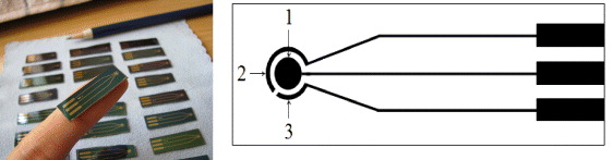
Figure 3 Schema of interdigitated array (IDA) with 1 - working electrode, 2 - reference electrode and 3- counter electrode.
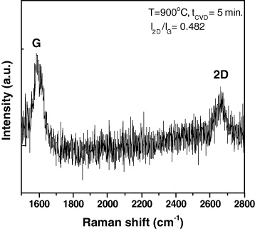
Figure 4 Raman spectrum of the graphene film grown on Cu tape at a temperature of 900 °C.
To estimate the thickness of the graphene film, the graphene film from the Cu tape was transferred to silicon substrate and the difference in the height of the graphene film and the silicon substrate was measured by AFM. The AFM image showed that the thickness of the graphene film was about 5 nm (figure 5), meaning that the grown graphene is multilayered (about 15 layers).
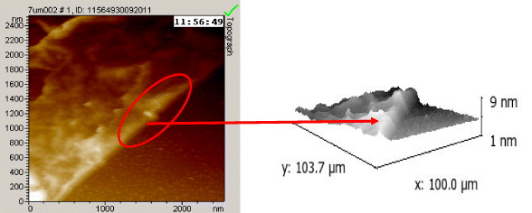
Figure 5 AFM image of the graphene film after transferring from Cu tape to silicon substrate.
3.2. Graphene transferring onto IDA
Transfer process of the graphene to IDA is described as follows: Firstly, a thin layer of polymethyl methacrylate (PMMA) was coated on top of obtained graphene films on Cu tapes. Then, the samples were annealed at 180 °C in air for 1 min. Subsequently, the graphene/PMMA films were released from the Cu tapes by chemical etching of the underlying Cu in an iron (III) nitrate solution. Then, suspended films were transferred to deionized water to remove the residual of Cu etching process. Next, graphene/PMMA films were transferred onto IDA electrode. For the purpose of better contact between the graphene film and the IDA electrode, an appropriate amount of liquid PMMA solution was then dropped on the cured PMMA layer for partially or fully dissolving the precoated PMMA. The re-dissolution of the PMMA tends to mechanically relax the underlying graphene, leading to a better contact with the IDA electrode. Finally, the PMMA films were dissolved by acetone and the samples were cleaned by rinsing several times in deionized water.
Some observations can be made from a field emission scanning electron microscopy (FESEM) image of graphene/Fe 3 O 4/PANi films (figure 6). First, it shows a spongy and porous structure of PANi, which in turn can be very helpful for enzyme trapping. Second, doped core-shell Fe 3 O 4 NPs (with a diameter core of about 30 nm) could also contribute to further immobilization of biomolecule, owing to their carboxylated shell. Furthermore, a thin and opaque graphene layer was distinguishably seen on the top of the electrode surface.
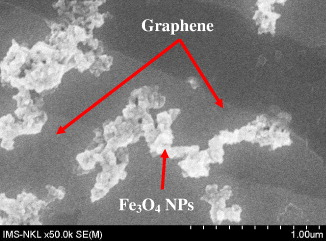
Figure 6 FESEM image of graphene/Fe 3 O 4 – doped PANi film.
3.3. Electrochemical behavior of graphene/Fe3 O4/PANi/GOx sensor
The behavior of each layer of the sensor was investigated by SWV. In figure 7 line 1 is the SWV signal corresponding to graphene/Fe 3 O 4/PANi film while lines 2, 3 and 4 are SWV curves of layer-by-layer IDA, corresponding to successive addition of glutaraldehyde, GOx and glucose, respectively. It is very interesting to note that while the electroactivity drops gradually from line 1 to line 3 (adding insulated components onto surface electrode), it increases in the upward direction from line 3 to line 4, along with glucose injection. Based on this signal-on phenomenon, highly sensitive detection of glucose can be expected.
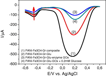
Figure 7 SWV curves corresponding to each layer formation.
3.4. Glucose determination
Figure 8 shows a typical current–time plot for the sensor at +0.7 V during successive injections of glucose (3 mM increased injection, at room temperature, without stirring, air saturated, in 50 mM phosphate buffered solution).
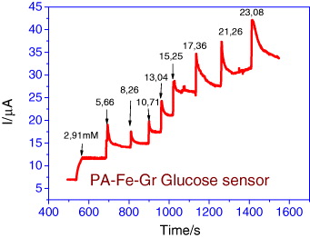
Figure 8 Amperometric responses to different added glucose concentrations.
The calibration plot indicates a good and linear amperometric response to glucose within the concentration range from 2.9 to 23 mM (with regression equation of ΔI (μA)=1.484 *C (mM)+6.764, R2=0.9969) (figure 9).
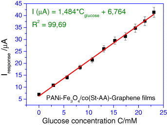
Figure 9 Glucose calibration line and respective regression equation.
Thus, with a miniaturized dimension (500 μm) the above graphene patterned sensor has shown much improved sensitivity to glucose, as high as 47 μA mM −1 cm −2 compared to a non-graphene one (10–30 μA mM −1 cm −2, as previously reported in literature [1, 5, 16]).
4. Conclusion
Graphene films (with about 15 layers) were successfully synthesized and transferred onto IDA surface for electrochemical detection of glucose. Graphene patterned interface and the ability to precisely control each layer are considered to be the main reasons enhancing significantly the sensitivity of this sensor. Its miniaturized dimension is also another attractive advantage that is worth further exploring in the future.
Acknowledgments
Funding of this work was provided by Vietnam Ministry of Science and Technology (grant 08/2011/HĐ-NĐT), National Foundation for Science and Technology Development (NAFOSTED grant 103.03.47.09) and IMS key Laboratory for Electronic Materials and Devices project (grant HTTĐ01.12). The authors also acknowledge VAST Scientific Council of Materials Science for additional financial support and Managing Board of Key Laboratory for Electronic Materials and Devices, IMS for providing their facilities.