
Abstract
Graphene, a carbon material discovered in 2004 by a group of scientists at the University of Manchester, UK, has been attracting significant attention in both fundamental and applied studies. Due to the rapid increase in the number of articles on this material since its discovery, a range of readers, particularly those just beginning to learn about this material, are turning to various different sources. The purpose of this article is to create a bridge between the key aspects of this material in experimental and theoretical investigations, as well as in fundamental and applied studies, aiming to provide a basic understanding of this material for those who are new to it. The presentation in this article is thus not particularly academic. The content focuses on four themes, including fabrication methods, basic properties, potential for application and some typical research directions for this magic carbon material.
Export citation and abstract BibTeX RIS

Content from this work may be used under the terms of the Creative Commons Attribution-NonCommercial-ShareAlike 3.0 licence. Any further distribution of this work must maintain attribution to the author(s) and the title of the work, journal citation and DOI.
1. Introduction
Carbon nano-materials are extensively studied nowadays since the discovery of fullerene molecules and particularly when graphene, a single layer of carbon atoms packed into a two-dimensional honeycomb lattice, was demonstrated to exist in 2004. Carbon has been known and used since ancient times as charcoal, one of its most common allotropes in nature. Murals on the walls of various caves in the world are evidence of the use charcoal (and other materials, of course) by human ancestors as an important tool in communication and/or the expression of the spirit. When people became interested in minerals under the earth, graphite was discovered and became commonly used, especially during the water–vapor period, wherein hard coal was a powerful fuel for operating water–vapor machines. Graphite has a rather special crystalline structure wherein carbon atoms bind strongly together in layers of two dimensions, but quite weakly among such layers. Because of this fact, graphite has been widely used for a long time ago as the writing point of pencils [1]. During the Cold War, this material attracted strong attentions as one that can lower the speed of neutrons in controlling the rate of nuclear reactions. From time to time, different elegant structures of carbon have been found, such as fullerene molecules in 1985 [2], carbon nanotubes in 1991 [3] and graphene in 2004 [4]. These discoveries resulted in a Nobel Prize and may generate another one in future. Physically, the finding of graphene filled in the last vacancy in the family of carbon allotropes according to their dimensions: fullerene (zero dimensional), carbon nanotube (1D), graphene (2D) and graphite (3D).
Theoretically, single graphite layers were studied a long time ago [5], but they just served as the starting point for graphite. Such special atomic layers were thought of as unable to exist in a freestanding form. Landau and Peierls argued that strictly 2D crystals were thermodynamically unstable and could not exist [6, 7]. Their theory pointed out that a divergent contribution of thermal fluctuations in low-dimensional crystal lattices should lead to displacements of atoms that are comparable to interatomic distances at any finite temperature [8]. The argument was later extended by Mermin [9] and was strongly supported by many experimental observations. The basic reason for this is that nature strictly forbids the growth of low-dimensional crystals [10]. Actually, the process of crystal growing usually implies high temperatures and, therefore, thermal fluctuations that are detrimental to the stability of macroscopic 1D and 2D objects. One can grow flat molecules and nanometer-sized crystallites but, as their lateral size increases, the phonon density integrated over the 3D space available for thermal vibrations rapidly grows, diverging on a macroscopic scale. This forces 2D crystallites to morph into a variety of stable 3D structures. The impossibility of growing 2D crystals does not actually mean that they cannot be made artificially. One can grow a monolayer inside or on top of another crystal (as an inherent part of a 3D system), and then remove the bulk at sufficiently low temperature such that thermal fluctuations are unable to break atomic bonds even in macroscopic 2D crystals and mould them into 3D shapes.
Though there are already several articles [10–14] reviewing remarkable progress in the research of graphene and of various patterns of this material, these focus strongly either on theoretical or experimental aspects, or are presented in a very academic way that generally requires a deep background knowledge and high relevant qualifications to understand their contents. Our approach here, however, is for beginners (i.e. scientists having little experience in either theoretical or experimental studies). Accordingly, our aim is to bridge between fundamental aspects in both experimental and theoretical studies. We hope that this will provide readers who are new to graphene with a short overview on basic knowledge that has been rapidly established since the discovery of this material. The paper is organized as follows. In section 2, several experimental aspects of how graphene was isolated and observed are reviewed, wherein the scotch-tape method—a handcraft manner of the top-down approach—is presented in section 2.1. Then section 2.2 introduces several methods based on the bottom-up approach that have been optimistically expected to overcome current technical challenges. In section 3, we present the electronic band structure of pure graphene and of its 1D strips or so-called nanoribbons. In this section, the calculations are presented in detail with the aim of providing the readers basic and specific aspects of the theoretical study and thus helping to explain the formation of today's 'graphene-rush'. Next, in section 4, we summarise key studies of the great potential of graphene for advanced applications in the future. Finally, several results in our recent studies are briefly presented in section 5 and our conclusions are presented in section 6.
2. Fabrication methods
2.1. Scotch-tape cleavage: the original method, the top-down approach
In 2004, a group of scientists at the University of Manchester in the UK led by Geim made a report in Science on their first success in isolating single layers of graphite, or graphene, as well as several anomalous properties of such layers. In supplementary material to their work, details of their technique were presented. According to this, the isolation procedure was realized by using 1-mm-thick platelets of highly oriented pyrolytic graphite (HOPG) as the initial material. A mesa was then covered on top of the platelets using dry etching in oxygen plasma. The structured surface was then pressed against a thick layer of a fresh wet photoresist spun over a glass substrate. By heating appropriately, the mesas became attached to the photoresist layer, which allowed them to cleave the mesas off the rest of the HOPG sample. They then simply used scotch tape to repeatedly peel flakes of graphite off the mesas. Thin flakes left in the photoresist were then released in acetone. Next, in order to observe and characterize the obtained graphite flakes, they need to be deposited onto the surface of appropriate substrates. Usually, the wafers of strongly n-doped Si are used for this. In the work of Geim's group, the silicon substrates with a thick layer of SiO 2 on top were used to avoid accidental damage, especially during the plasma etching process. The substrate was simply dipped into the obtained solution to attach the resulting flakes onto its surface, which was then washed in plenty of water and propanol to remove the thickest flakes. This cleaning process was then refined using ultrasound in propanol. The thick graphite flakes of thickness less than 10 nm were demonstrated to be strongly attached to SiO 2 due to Van der Waals and/or capillary forces.
As indicated by Geim, graphene can be easily made but is difficult to detect [10]. However, now there are several effective methods to do so, for example, by analyzing basic anomalous properties of graphene, such as observing the quantum Hall effect or analyzing the Raman spectrum. At the beginning, Geim and his co-workers had to make a complex combination of different observations. In a paper published in Nature Materials, Katsnelson interestingly commented that graphene sheets are created any time we use a pencil for writing, but with the naked eye we are not aware of their presence [15]. Geim and Novoselov [10] combined optical, electron-beam and atomic-force microscopy to detect graphite films of several layers. Graphitic films are transparent to visible light even with a width of 50 nm. Nevertheless, on the SiO 2 surface, they are quite easy to see due to the added optical path that shifts the interference colors. The color for a 300 nm wafer is violet–blue and the extra thickness due to graphitic films shifts it to blue. At thicknesses d≲1.5 nm, as measured by AFM, graphene films are no longer visible even via the interference shift as they become too thin. Taking advantage of this fact, the graphene films in their work were selected as those that were completely invisible in an optical microscope (OM) but can be seen in a high-resolution SEM. The few-layer graphene (FLG) film gives a clear contrast in SEM but would be impossible to see in OM if an isolated FLG film were shown. AFM was then extensively used to measure the thickness d of FLG films. In most cases, they observed that d ranged from 1 to 1.6 nm while the interlayer distance in bulk graphite was about 3.35 Å. This shows that FLG films were indeed only a few atomic layers thick. However, it should be remembered that the distance estimated from AFM measurements includes the distance between the graphene layer and the SiO 2 surface. Using SEM, they observed that the FLG films were rarely completely flat but some areas were ruptured and folded back. They also detected a step height of ≈4 Å in such films. This value is in good agreement with the step height (d≈4 Å) measured for 'nano-graphene' on top of HOPG. Accordingly, this shows that such films are indeed single-layer graphene sheets.
We have presented a short description of how single-layer graphene sheets can be isolated and detected. Basically, fabrication is based on the fact of very weakly binding between graphite layers. That explains why this method of lifting graphite layer by layer is referred to as the scotch-tape technique. By improving several intermediate steps, this method allows the production of large graphene sheets, even in millimeter sizes, and with high structural quality. The method is therefore still commonly used for basic research and is ideal for making proof-of-concept devices in the foreseeable future [14], and further developments have been made to improve the consuming time and the yield [16, 17].
2.2. Large-scale and yield methods, the bottom-up approach
Though the mechanical method can be improved to produce a large yield of graphene, the obtained graphene is usually in the suspended state and is of submicrometer size. In electronic applications, such graphene sheets are not suitable to be manipulated to make complex devices and integrated circuits. Required graphene should be large, in the centimeter scale and flat enough. The scotch-tape method obviously reveals a great limit in this sense. Accordingly, alternative ways should be found and developed to satisfy such requirements. So far, there are two approaches that have been rapidly developed and are expected to overcome such challenges. The first is epitaxial growth based on chemical vapor deposition (CVD). The second is based on the decomposition of different materials, such as silicon carbide (SiC). As mentioned above, since nature does not favor growing small crystals, in order to grow graphene one should use appropriate substrates to avoid thermal fluctuations that could break the crystalline structure of samples. This is 3D growth since during the process graphene always binds to the underlying substrate and therefore suppresses bond-breaking fluctuations. After cooling down the epitaxial structure, the substrate can be safely removed by chemical etching. Until now, a lot of effort has been made and graphene has been successfully grown on the surface of different metals, such as nickel (Ni) and copper (Cu). For instance, Reina et al [18] used the CVD method to grow graphene on polycrystalline Ni films and obtained single-layer and few-layer graphene sheets of centimeter-scale width. They also claimed that their method is low cost and scalable. However, the graphene layer number was not controlled in their synthesis process. Kim et al [19] grew graphene sheets on thin Ni layers and then successfully transferred them to arbitrary substrates. They pointed out that single-layer graphene sheets transferred to SiO 2 substrates have a good electron mobility value, which could be improved to be greater than 3700 cm 2 Vs −1 at low temperature—very close to that of cleaved graphene. In particular, a pronounced half-integer quantum Hall effect was observed. Using a different substrate, i.e. copper instead of nickel, Li et al [20] synthesized a large area at high quality as well as uniform graphene films. Compared to other groups, Li et al have achieved significant progress when using methane in their synthesis process and mainly obtained single-layer graphene sheets with a quite small percentage (<5%) area of few-layer graphene. As shown in [20], the obtained graphene sheets are quite smooth and continuous across the copper foil surface. The sheets were well transferred to Si/SiO 2 substrates and at room temperature they showed high electron mobility of about 4050 cm 2 Vs −1.
Recently, silicon carbide (SiC) has attracted special attention. Indeed, single- and few-layer graphene can be created by decomposing this material by heat. The benefit lies in the fact that the resulting graphene automatically lies on an insulating substrate, i.e. one does not need to transfer the graphene sheet on to the other substrate as in metal-catalyst epitaxial growth, and in principle there is no limit to the size of the graphene sheet created. However, according to Geim [14], one should distinguish the kinds of graphene sheets formed on the surface of a SiC substrate. Because of the organization of silicon and carbon atoms in such substrates, there are two scenarios that graphene sheets can be grown in. The first is that a single- or double-layer graphene sheet is grown on the Si-terminate face. In the second case, a multi-layer sheet is rapidly grown on the carbon-terminal face. As demonstrated by Emtsev et al [21], the annealing environment is very important to obtain good-quality graphene sheets. Using an argon atmosphere, they dramatically improved the uniformity of the graphene layers, which thus yielded nice transport characteristics. For instance, the typical linear picture of the graphene spectrum can be retained for the energy range higher than ∼0.3 eV since a small energy gap of 0.26 eV is opened up [22]. This fact is very interesting and the origin of such an energy gap is obviously due to the binding between the resulting graphene sheet and the substrate, which would lead to strong doping (∼1013 cm −2) of the sheet. In a recent article entitled 'Epitaxial graphene: how silicon leaves the scene?', published in Nature Materials, Sutter [23] highly appreciated the efficiency of this method and mentioned to a bright prospect of a new era of graphene in electronics rather than silicon.
Apart from the size issue of the graphene sheets, the fabrication yield is also raising as a great requirement. In 2008, Hermandez et al [17] announced a method that allows the production of graphene with a high yield. The method is based on the dispersion and exfoliation of graphene in organic solvents such as N-methyl-pyrrolidone. Since the surface energies of this solvent match that of graphene and the solvent–graphene interaction is balanced with the exfoliation energy, they successfully demonstrated graphene dispersions with concentrations of up to 0.01 mg ml −1. Single-layer graphene was confirmed to be present and was characterized by Raman spectroscopy, transmission electron microscopy and electron diffraction. It is very interesting to note that the resulting single-layer graphene sheets by this method are defect-free. The authors even emphasized that their method can be improved to increase the yield from 1 wt% to 7–12 wt%. Different chemical methods have commonly been used. In a short, but quite impressive, article in Nature Technology [24], Ruoff suggested that all chemists should have an appropriately positive and active attitude towards graphene. Choucair et al [25] suggest that though single sheets of pristine graphene have been isolated from bulk graphite in small amounts by micromechanical cleavage, and large amounts of chemically modified graphene sheets have been produced by a number of approaches, both of these techniques require highly oriented pyrilitic graphite and have to suffer several stages. They therefore developed a direct chemical synthesis of single-layer graphene sheets in gram-scale quantities. Their approach is bottom-up, using ethanol and sodium to directly obtain sheets, and they are dispersed by mild sonification.
In spite of such successes, one of the big problems of large-area single-layer graphene sheets is their structure [26]. Such graphene sheets can be well dispersed but they still are not perfectly flat. In the epitaxial growth methods, graphene sheets have to be transferred to an appropriate substrate and are usually observed to be corrugated. Anyway, it is worth acknowledging the great efforts of scientists in making graphene evolve rapidly since its discovery in 2004.
3. Electronic properties
Though graphene was just discovered six years ago, its electronic properties had been studied for a long time previously. The research was done with graphite, an important material in nuclear reactors strongly developed during the Cold War [5, 27, 28]. Based on the electronic structure, some anomalous phenomena observed in graphene, such as the half-integer quantum Hall effect, and the quantization of the electronic conductivity [4, 29], have been correctly explained. In several recent reviews [12, 30, 31], the electronic picture of this material was always presented in a large volume of articles. It is through this electronic picture that one can appreciate the typical and unique properties of this novel material. For instance, the behavior of electrons in this material rather mimics that of relativistic particles, thus several problems arise, e.g. the Klein paradox, in the domain of high-energy physics, has been expected to be verified through in-lab experiments with graphene. Though this fundamental knowledge is rather commonly presented, we decided to spend a sufficient volume of this paper to introduce key points about the electronic structure of this material and of related one-dimensional patterns. It should be emphasized that the following presentation is not a complete lecture on the electronic structure but we aim at the pedagogical meaning of using this material as a typical example to highlight various physical concepts in condensed matter physics.
3.1. Electronic band structure of graphene
The honeycomb lattice structure of graphene is shown in figure 1, wherein the shortest distance between two carbon atoms is a cc ≈ 0.145 nm. To construct the reciprocal lattice, one first of all has to determine the so-called primitive cell from which, by translational symmetry, the whole lattice of graphene is recovered. Such a unit cell can be chosen as that denoted in figure 1 wherein the two unit vectors are denoted by a1 and a2. The unit cell is thus a lozenge, which on average consists of two lattice nodes, denoted by A and B. Based on these basic vectors, any lattice node, e.g. i, is totally determined by a vector R i =ma 1+na 2, where m and n are two integer numbers. Concerning other symmetries of the graphene lattice, it is straightforward to realize that the rotation by an angle of 60° around an axis perpendicular to the graphene sheet at any grid node does not change the lattice. One can also realize six mirror symmetrical planes that are perpendicular to the graphene sheet and consist of one of the six sides of a hexagon. There are also three other mirror symmetrical planes that consist of two middle points of the two opposite sides of the hexagon.
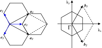
Figure 1 Illustrations of the honeycomb lattice and the Bravais lattice of graphene (on the left-hand side) and of the unit cell of the reciprocal lattice and the first Brillouin zone (on the right-hand side).
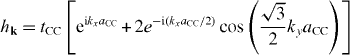
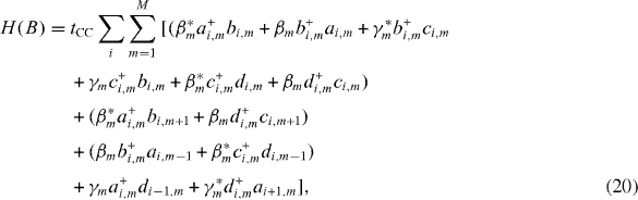
Now, in order to study the electronic band structure of graphene, we need to explicitly determine a Hamiltonian in an appropriate form. Since all σ-orbits of carbon atoms have been used to make strong bonds in the graphene plane, conductive properties of this sheet are governed by the π-orbits that are perpendicular to the graphene plane. As already proved, the electronic band structure of graphene can be described by using a simple tight-binding model [31]. We repeat below some calculations based on this approximation. To do so, first of all we denote ai + , bj + and ai , bj , the operators creating and annihilating an electron in the π-orbit of the A and B carbon atoms located at the grid nodes i and j. In the framework of the nearest neighbor tight-binding approximation, the Hamiltonian of conductive electrons in the graphene lattice reads

where t CC ≈−2.67 eV is the hopping energy between the two nearest lattice nodes, and h.c. refers to the Hermitic-conjugate term of the former. Because of the translational symmetry of the crystalline lattice, we can now Fourier transform the involved operators,

and then substitute them into the Hamiltonian expression. After some simple algebra, we obtain

wherein and the identity has been used. The above result can be written in the matrix form using a vector-notation for the creation/annihilation operators, i.e.
Under this convenient form, it is straightforward to diagonalize the Hamiltonian to obtain two energy dispersion relations E(k)=± |hk |. From the real lattice of graphene, we can specify coordinates of the three vectors ei(j)=Rj −Ri as follows:
Using them, it is easy to calculate
and therefore the energy dispersion expressions read
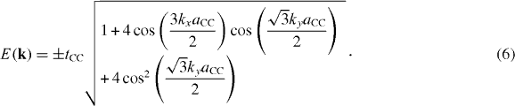
The energy dispersion relations, equation (

wherein v
F
is called the Fermi velocity whose value is just 300 times less than the speed of light, and are two of three well-known Pauli matrices. The Hamiltonian (

Figure 2 Three-dimensional display of the energy band structure of graphene, equation (

Figure 3 Two-dimensional contour display of the energy band structure of graphene showing clearly the hexagonal first Brillouin zone. The three most symmetrical points of this shape are noted.

Figure 4 The energy dispersion curves of graphene plotted for the wave vector along the directions noted in figure 2 (the square triangle). Around the K-point, the energy dispersion curves can be linearly fitted, implying the low energy excited states as massless Fermion particles.
Recently, graphene was epitaxially fabricated on SiC substrates. The obtained material is very different from that created via the exfoliation method; the electronic structure of epitaxial graphene there appears an energy gap. Measurements reported that such a gap is about 0.25 eV [22]—much smaller than usual gaps in some common conventional semiconductors (∼1 eV), but ten times larger than the thermal energy at room temperature (300 K). Accordingly, the Hamiltonian for the low energy excited states around the K-points in the epitaxial graphene should be modified from that of isolated graphene by adding a mass term. Such a Hamiltonian should have the form

We have developed techniques to study this Hamiltonian. We suppose that, in the effective modeling viewpoint, this model is a good starting point to study further applicable potentials of graphene in future.
3.2. Electronic band structure of graphene nanoribbons
3.2.1. Zigzag-edge graphene nanoribbons
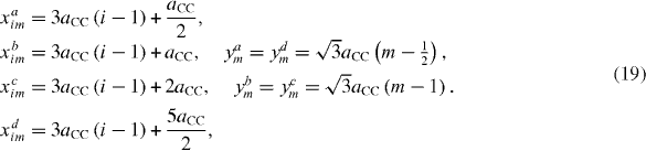
The first observations of graphene flakes fabricated by the scotch-tape method by Novoselov et al evidently pointed out the geometrical shape of the edge of graphene sheets. The high solution SEM images typically show that the edge of a graphene sheet can be either zigzag-shaped or armchair shaped, or a mixture of both. In this subsection and in the next one, we will present the electronic band structure of only the two typical ribbons, one with the edges in the zigzag form and another in the armchair form. In figure 5, we illustrate a schema of a zigzag-edge ribbon. Geometrically, any ribbon is characterized by two parameters—the width and the length—which are determined through the zigzag line number along the ribbon length and the unit cell number as
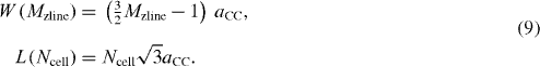

Figure 5 Schematic illustration of zigzag edge graphene strips. The super-unit cell is marked by the green box. The positions of carbon atoms are coded and also presented.
In figure 5, the super-unit cell is marked by a rectangular box, which consists of an armchair line of carbon atoms along the transverse direction. The rule of positioning each atom in the super-unit cell is also illustrated in the figure. Besides the translational symmetry along the length of the ribbon, depending on the zigzag line number, the ribbon may possess a mirror symmetry with the mirror plane perpendicular to the ribbon sheet and consisting of its axis.
Though the nearest-neighbor tight-binding approximation predicts the electronic structure of graphene, there are some limitations when using it for graphene nanoribbons, details of which are in [12]. However, this approximation is still a powerful and efficient method that can provide a lot of important information. Practically, the method is usually used to obtain rough information about the energy band structure as well as the transport properties of various nanoscale systems. To additionally highlight the pedagogical meaning of graphene that we mentioned at the beginning of section 2, the nearest-neighbor tight-binding model is used again to derive the energy band structure of the two mentioned kinds of graphene ribbons. Obtained results will also compared to those obtained by other precise methods to show the limitations of the used method.
In the case of the zigzag edge graphene ribbons, a nearest-neighbor tight-binding Hamiltonian takes the form
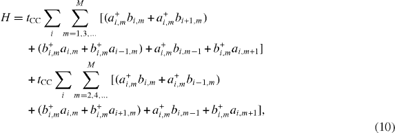
wherein all of the involved notations are similar to those referred to as in the case of graphene. This model can be expanded to include the effects of a uniform magnetic field normalizing the plane consisting of the ribbon by changing locally the hopping energies using the Peierls substitution. Using the Landau's gauge

the magnetic field-dependent hopping energies are determined as
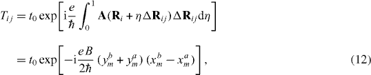
where
Setting wherein , the tight-binding Hamiltonian is then written down in the form
Now taking the Fourier transform of all of the operators,
the first Brillouin zone can be determined as all possible values of k satisfying the condition
After some tedious calculations, we arrive at a simple expression of the Hamiltonian,
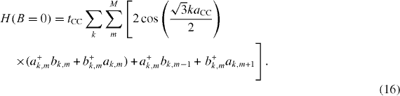
which in the case of the system without a magnetic field becomes
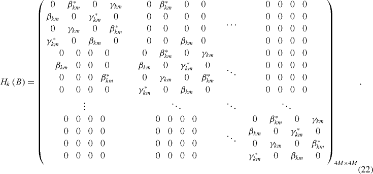
For the convenience of calculation, the above results should be encoded in the matrix form. The k-dependent Hamiltonian therefore reads
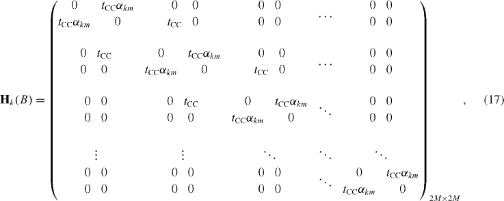
wherein
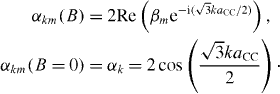
For each value of B, diagonalizing the above matrix, equation (
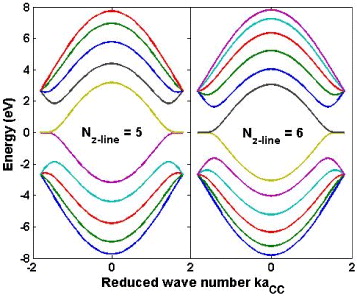
Figure 6 Electronic band structure of the two zigzag edge graphene ribbons with the zigzag line number of 5 (left panel) and 6 (right panel), showing a picture of no energy gap.
3.2.2. Armchair-edge graphene ribbons
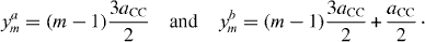
Concerning graphene ribbons with the edges in zigzag shapes, theoretically there are two kinds of ribbons, one with a defined armchair line number M aline along the ribbon length (illustrated in figure 7), and another without it. Besides the translational symmetry along the ribbon length, there exists a quasi-mirror symmetry plane with the length of a glide vector of 2a CC for the former ones, but a true mirror symmetry plane for the latter ones. However, for the electronic structure, in the following we only focus on the former one whose width and length are determined by

Figure 7 Schematic illustration of armchair edge graphene strips. The super-unit cell is marked by the green box. The positions of the carbon atoms are coded and also presented.
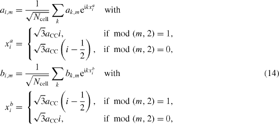
The super unit cell of the considered armchair-edge ribbons is highlighted in figure 7 by a blue rectangular box. The carbon atoms in the super unit cell are coded as in the figure and their positions are determined by
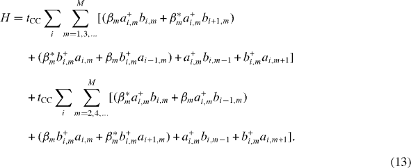
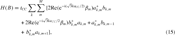
Using the same Landau gauge as presented in the previous subsection, the nearest-neighbor tight-binding Hamiltonian depending on a magnetic field is written in the form
where
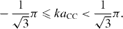
Taking the Fourier transform of all involved operators with respect to the cell index, we can determine the first Brillouin zone of the energy band structure as -(π /3) ≤ka CC < (π /3). After some tedious calculations and by setting β km =β m e -i(ka CC /2) and γ km =γ m e -i ka CC , we arrive at the Hamiltonian
The k-dependent Hamiltonian, which is needed for the calculation of the band structure, is then written in the matrix form as
In figure 8, we present the energy band structure for a typical armchair-edge graphene ribbon of width 1.5 nm under a zero-magnetic field. The nearest-neighbor tight-binding calculation presented above, in this case, predicts the appearance of a finite energy gap, implying that the considered graphene ribbon is a semiconductor. This simple calculation scheme actually fails in some cases when predicting them as semi-metals, which is in contrast to experimental data [36] and other calculation methods from first principles [12]. Accordingly, the nearest-neighbor tight-binding calculation should be used only to qualitatively illustrate the electronic properties of the armchair-edge graphene ribbons; however, it is still good enough in the case of graphene and zigzag-edge ribbons.
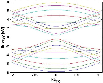
Figure 8 Electronic band structure of an armchair-edge graphene nanoribbon of width 1.5 nm. The nearest-neighbor tight-binding calculation predicts a finite energy gap, different from the case of the zigzag-edge ribbons.
4. Applications
4.1. Composite materials
The well-known one-dimensional carbon nanotube has been widely studied since its birth in 1991 due to its mechanical robustness and its unique electronic properties. It can be said that fundamental studies have rapidly made mature this one-dimensional carbon material and increasing potential for applications in various areas such as composite materials, gas sensors, electronic and spintronic devices. So far, there are several methods commonly used to fabricate carbon nanotubes, such as chemical-vapor deposition (CVD) and thermal-mechano [37] methods. These methods, however, are expensive and/or less efficient, for instance, for usage in composite materials. In this sense, the appearance of graphene by the exfoliation method becomes very remarkable since such a manual method is clearly simpler and cheaper than traditional methods used to produce carbon nanotubes. As demonstrated by Stankovich et al [38], the conductivity of conductive plastics can be significantly improved just by filling graphene powder about just 1% of volume; however, the mechanical strength of such composite materials may be less than that made from carbon nanotubes.
In the battery industry, graphene also has great potential due to its natural properties, i.e., planar structure, high electric conductivity and very large surface-to-volume ratio, as well as its cheap cost of production. In this sense, this material is even able to replace carbon nano-fiber, a material commonly used in the battery technology today, and consequently, the efficiency and price of batteries may be significantly improved.
Another aspect that should be addressed when considering graphene for composite material application is its potential for hydrogen storage [39] and gas sensors [40] due to the very large surface-volume ratio and the pz orbital perpendicular to the graphene surface. Accordingly, various kinds of gas atoms, not only hydrogen, can be easily absorbed on graphene by making bonds with such pz orbitals. Practically, this is one of the most attractive directions of research.
4.2. Electronics: beyond current CMOS devices
It can be said that one of the most important reasons behind graphene becoming so attractive is its application potential in electronics and spintronics. As mentioned in this paper and in other sources, due to unique properties such as the stability of even nano-scale graphene sheets, the large mobility of charges, and the ease of doping by the field effect, this two-dimensional carbon material seems to satisfy many requirements beyond silicon technology. Though it cannot disclaim the crucial role of silicon in our world today, one has become aware of the limitations of this material. To understand why graphene has been welcomed right after its birth, it may be helpful to take a look at the development tendencies of the current technology. Basically, it is at the forefront of going on to reduce the size of built-in-block devices, such as diodes and transistors, in integrated circuits to the nanometer scale while still ensuring the correct operation of such devices. Quantum mechanics principles, however, tell us that surely there is a scale limit below which everything becomes 'collapsed'. Indeed, at the nano-scale, the device sizes can be comparable to one of physical lengths such as the mean-free path and/or the phase coherent length; quantum effects therefore emerge and they usually tend to erase the required characteristics of devices. For example, when the channel length of a metal oxide semiconductor field-effect transistor (MOSFET) structure is reduced, carriers (electrons and/or holes) can easily tunnel through a potential barrier in the channel region, which is controlled by gate voltages, leading to an increase in the threshold voltage and the sub-threshold swing, and a decrease in the ratio of the current values at the ON to OFF states. Generally speaking, scaling device sizes leads to the appearance of so-called short channel effects, which deviate or even change the current–voltage characteristics of the device and also increase the power consumption due to thermal dissipation. The improvement in these properties requires simultaneously reducing the thickness of the insulator layers, which separate the semiconductor channel from the gate leads, and that of the semiconductor channel itself. Unfortunately, reducing normal semiconductor thickness usually brings about the degradation of the charge mobility. For instance, for a silicon layer of width 0.7 nm, the charge mobility is just 70 cm 2 Vs −1 [41]. However, graphene usually exhibits very high charge mobility. For instance, the value μ=15 000 cm 2 Vs −1 can be measured in most available graphene samples at room temperature. This value is obviously comparable to that of the best Si samples at low temperature known today. More interestingly, it was also found that this quantity weakly depends on the temperature, and it is very easy to change and to control the type of carriers in the graphene sheets just by using an electrostatic field. This fact is known as the doping using the field effect, which can also be used for carbon nanotubes.
One of the big obstacles of graphene for applications in electronics is that this material is a semi-metal, not a semiconductor. As demonstrated in section 2, the band structure of an ideal graphene sheet has no energy gap. It therefore causes difficulties in controlling the charge carrier density and therefore the current of charges flowing through graphene channels in devices. As an example, the negative differential resistance was predicted in the current–voltage characteristics of a single gate graphene structure but it is not enough for applications as the resonant tunneling diodes [42]. The reason was given as due to the transition of charges from the valence band to the conduction band, and vice versa; the picture looks similar to the band-to-band tunneling which makes the current rapidly increase versus the bias. Engineering a graphene electronic structure is therefore currently an intriguing research direction. Essentially, the fact of gapless graphene is due to the equivalence of the two triangular sub-lattices composing the honeycomb one. Naturally, in order to separate the upper and lower energy bands from the K-points, one needs to break this equivalence. Different from a single layer of carbon atoms, the so-called bilayer graphene possesses an energy gap of about 0.3 eV. In this material, the two single graphene layers stake together in the Berry type and therefore break the mentioned equivalence. A finite energy gap can also be created in single-layer graphene by spatial confinement or lateral-superlattice potential. The latter seems to be a relatively straightforward solution because sizeable gaps (>0.1 eV) should naturally occur in graphene epitaxially grown on top of crystals with a matching lattice, such as boron nitride or SiC [43–47], in which large superlattice effects are undoubtedly expected. For the former, Nakada, Brey and Son and their co-workers predicted that an energy gap would be observed for graphene nanoribbons. Moreover, they also pointed out that such an energy gap is inversely proportional to the ribbon width [48–50]. This prediction was then confirmed by Han et al, who experimentally showed that law [36]. Accordingly, in order to have band gaps comparable with those of common semiconductors, it is required that semiconductor ribbons should have widths of less than 10 nm [36, 50]. Unfortunately, current technologies cannot controllably fabricate such ribbons with a precision at the atomic scale at the edges. The edge roughness is a severe problem that may cause charge localization and therefore reduce strongly the conductivity [51, 52].
Now there are already several efforts to improve the perfection of ribbon edges [53–56] but they seem to still be far from reaching the atomic scale precision for nice properties of nanoribbons. Irrespective of that, several MOSFET prototypes have been demonstrated. For example, Ponomarenko et al in 2008 [57] argued that their devices based on graphene quantum dots larger than 100 nm can operate well as single-electron field-effect transistors (FETs), exhibiting periodic Coulomb blockage peaks. However, they pointed out that this picture became irregular in devices with a dot size smaller than 100 nm due to the randomness of the edges and the importance of quantum confinement. Li et al [53] from Stanford University reported on the characteristics of their MOSFETs based on graphene ribbons with a width of about 10 nm and the ON–OFF ratio up to 107, but the saturation regime is not seen as in conventional devices. Recently, Lin et al [58] from IBM proclaimed in Nano Letters that their devices can operate well at a frequency up to the gigahertz scale and are virtually noiseless. A cutoff frequency of 26 GHz was reported for a structure of 150 nm gate length and was pushed up to 100 GHz early in 2010. These efforts are clearly extremely meaningful in attracting great attention and motivating further steps towards the realization of graphene-based electronics for high-frequency applications.
According to Geim (see, for instance, [14]), due to the absence of experimental tools to determine structures with atomic precision, one should not consider graphene as a new channel material for FETs, but as a conductive sheet in which various structures of nanometer size can be carved to make single-electron-transistor (SET) circuitry. This idea actually had been experimentally proved by Geim and co-workers [57]. Though the SET architecture has been relatively well developed using Si-based technology [59, 60], it has limitations due to difficulties with the extension of its operation at room temperature. The main reason lying in the Si-based technology is the poor stability of conventional materials under nanometer sizes. However, architectures built in graphene are very stable in the nanometer scale and even in the much smaller molecular scale as single hexagonal or benzene rings. Very recently, for example, by using an electron beam irradiating a graphene film, a chain of carbon atoms was stably demonstrated [61]. Taking advantage of this fact, in Ponomarenko's work, the top-down approach was used to cut graphene sheets into complete SET structures including quantum dots—the device active region, barriers and interconnects. Though graphene-based SETs had been conceptually demonstrated, there are basically two big challenges that one should consider in proposing applications. Despite progress in the epitaxial growth of graphene [46, 47], the first challenge is fabricating larger and higher-quality wafers on an industrial scale. The second is the need to control individual features in graphene devices accurately enough to provide sufficient reproducibility in their properties. This point is also the same challenge that Si technology has been facing. For the time being, proof-of-principle nm-size graphene devices should be made by electrochemical etching using scanning-probe nanolithography [62].
4.3. Spintronics and other innovative researches
Spintronics is a field of research focusing on effectively controlling and manipulating the spin of charge carriers in solid-state systems [63]. Because of the very long mean-free path of electrons and the very weak spin-orbit coupling, graphene is currently considered as an ideal material for spin conduction [64–66]. A structure of a two-electrode spin valve fabricated by Hill et al [65] using a single layer of graphene shows a magnetoresistance (MR) of up to 10% at 300 K, a remarkably large value. Tombros et al [64] also reported the observation of spin transport and the Larmor spin precession over distances of several micrometres in single-layer graphene sheets. Cho et al [67] performed nonlocal four-probe spin valve experiments on graphene contacted by ferromagnetic Perm alloy electrodes and observed at 300 K a sharp switch and often the sign reversal of the non-local resistance at the coercive field of the electrodes. This observation apparently indicates the presence of a spin current flowing between the injector and the detector. Besides the recycling of characteristics of graphene-based conventional devices, innovative structures have also been under design to exploit the unique and robust properties of this material. Based on the fact that there are two inequivalent Dirac points (valleys) in the energy spectrum of graphene and the virtually absent intervalley scattering in pure graphene samples, Recerz et al [68] proposed a structure, namely the valley filter, which functions similarly to the spin filter as commonly known in spintronics. The two valley filters used in series therefore may operate as a valley valve. This proposal may open up a new area of research of the so-called 'valleytronics'. Together with progress in technology and in an understanding of graphene, this direction of research is probably becoming realistic and would have a deep impact on future technology.
5. Some research topics
The purpose of this section is to present research topics that we have been pursuing as well as several important results we have obtained. Inspired by the 'graphene rush', we became interested in this material in 2008. Our focuses are in electronics and spintronics wherein we explore possible potentials of this carbon material for advanced device applications. Though carbon nanotubes have been strongly studied for applications in electronics, they have been found to be not very compatible with current CMOS (complement metal-oxide semiconductor) technology due to difficulties in orienting such tubes. The discovery of graphene apparently provides a promising solution for future beyond-CMOS nanoelectronic devices because of its natural planar form. Some recent work has suggested that graphene devices might work at much lower supply voltages than those based on normal semiconductors today. Graphene is therefore expected to increase computing performance, with functionality and communication speed far beyond the expected limits of conventional CMOS technology.
The simulation of nanostructures and modeling of physical phenomena occurring at the nanoscale is crucial for the sustainable development of nanoscience and nanotechnology. Modeling the structural and electronics characteristics of nanodevices, such as graphene-field effect transistors, has been necessary to (i) provide a visual description of what really happens inside a nanodevice, (ii) optimize its performance and (iii) improve the understanding of nanoscale properties (physical, chemical and biological). In addition, the engineering and integration of new low-dimensional materials, such as carbon-based materials, along with the mastering of quantum phenomena emerging at the nanoscale, increasingly demands more realistic simulation of atomic-scale features of device components (material interfaces, chemical heterogeneity and conductance properties), as well as for more sophisticated treatment of quantum physics (interactions, many-body effects and out-of-equilibrium phenomena), which will ultimately dominate any underlying device characteristics, the design of novel functionalities and circuitry performance. However, sophisticated computational frameworks are scarce and not versatile enough. Often, the fundamental and spectacular properties revealed by state of the art ab initio methods are not transferable into realistic device simulation, and the lack of simplified models prohibits the study of essential statistical features, such as device variability.
Our first publication involving graphene is the article [42] wherein we developed a simulation tool based on the non-equilibrium Green's function theory, which was successfully applied to study the quantum transport of charges through resonant tunneling diodes (RTDs) and double-gate MOSFET structures [69]. The work focused on the treatment of the tunneling of quasi-particles in graphene through an electrostatic potential created thanks to an external gate electrode. As presented in section 2, the low energy excited states in graphene can be seen as massless Fermions that possess features of relativistic massless particles moving with a velocity just 300 times less than that of a photon. We numerically pointed out that such particles, if moving incidentally to the barrier interface, are not obstructed by any barrier potential in spite of its height and its width. This result is commonly known in Quantum Electromagnetic Dynamics (QED) as the Klein paradox, which was first discussed in graphene by Katsnelson in Science in 2006 [15]. However, different from Katsnelson's work, our data show that as a function of energy, the transmission probability for such particles, i.e. with a zero-incident angle, is not entirely identical to unity but oscillates slightly. Such oscillations actually reflect the confinement of the hole/electron states inside the potential barrier. Nguyen et al [70] exploited this point to study the spectrum of bound states in a potential barrier by studying the peaks of the transmission probability. Our work went further by predicting that if applying a voltage at one of two electrodes of the considered structure, the current–voltage characteristic may exhibit a negative differential resistant (NDR), an interesting feature commonly found in conventional semiconductor heterostructures such as RTDs. Though the NDR was first suggested by Dragoman and Dragoman [71], we later pointed out that the ratio of the current peak to the current valley is difficult to get a high value due to the fact of a very small or zero-energy gap [42]. Developing the idea of Haugen et al [72] of introducing a ferromagnetic state into a graphene sheet using the proximity effect, we investigated the polarization of spin currents, a main issue in spintronics. We predicted the oscillations of the conductance, and thus the spin-polarization, as a function of the barrier height, as well as the modulation of the latter quantity versus the barrier width. The polarization of the spin current was also studied. Simulation data showed that by tuning the gate voltage, one can switch from the up-spin current to the down-spin current and vice versa. This result is very interesting since it may be meaningful in future applications.
Realizing the imperfection of the flatness and the purity of real fabricated graphene sheets, we recently made a study of the influence of two typical scattering processes: one is due to the lattice defects or vacancies and another is due to impurities absorbed onto the graphene surface, which are virtually unavoidable. In that work [34], we pointed out that transport features of nanoscale graphene sheets are severely degraded if the scattering of relativistic-like massless Fermion particles on vacancies is dominant. In other words, it means that if the quality of the honeycomb lattice is low, e.g. if n vacancy >1011 cm −2, the mobility of charges may be suppressed, i.e. at low-energy, charges probably cannot transfer through a short distance of even several tens of nanometers. However, external impurities were found to affect the conductivity and the charge mobility more weakly than vacancies at the same density. Around the neutral Dirac point, a slight change in the conductivity was seen if the impurity density was higher than 1012 cm −2, but it was different at a higher Fermi energy range (see more details in [34]). Our model, though, is still simple; the obtained results are in good agreement with experimental data. In particular, we realized a typical distinction between these two scattering mechanisms, which may be used to highlight recent experimental data of the mobility of charges [34, 73, 74].
In other work [75], we continued focusing on the ability of controlling the spin-current in structures based on graphene nanoribbons whose edges are in the armchair pattern. The non-equilibrium Green's function method was still developed but, in this work, the Dirac model for low energy excited states was not used. Instead, an appropriate nearest neighbor tight-binding model for the graphene honeycomb lattice was considered to investigate the transport in the whole energy range. In particular, we studied the effects of the device–contact coupling by modeling the lead contacts in different ways. We predicted that the spin-polarization can get a very high value, ∼100%, by using an appropriate metal for contact leads. Our study therefore suggested that a device structure could be carefully designed to obtain high controllability of spin-polarization current.
6. Conclusions
Graphene is truly an amazing material. The discovery of this material, on the one hand, has virtually opened up a novel possibility in applied research beyond silicon-based CMOS technology but, on the other hand, it also challenges many technological problems to have specific applications. So far, many efforts have been made to understand various features of this material and to verify the correctness of different physical laws which have been established in various fields of physics, and to search possibilities of applying this material as well as associated novel physics in future technology. In this article, we have tried to carry out a brief overview of general basic knowledge of graphene and various patterns of this material, i.e. the nanoribbons. Due to the rapid development of technologies and fundamental research, it is difficult to keep up-to-date with all such progress. However, we have only focused on several aspects in fabricating graphene, aiming at bringing to readers an interesting history of how graphene was experimentally found, though theoretical predictions said not, and mentioning challenges in the current technology to synthesize large-scale graphene sheets at large yield and in high quality for real applications. Besides information and knowledge that can be obtained from direct observation of graphene samples, elegant and novel phenomena, such as the half-integer quantum Hall effect, and/or whether the existence of a universal minimal value of the conductivity can only be understood by studying in depth the electronic band structure of electrons in the honeycomb lattice of graphene. That is why a considerable part of the paper is devoted to the band structures of graphene and its one-dimensional patterns in section 3. Additionally, we have tried to give an overview of graphene and its one-dimensional patterns by presenting briefly several typical directions of the applied research that has been undertaken with some success.
Acknowledgment
One of the authors (VND) was financially supported by the Ministry of Education and Training, Vietnam, through project No B2009-01-286.