
Abstract
We demonstrate ZnO and In2O3 microcrystals as an optical probe for wide range thermometry. Both ZnO and In2O3 microcrystals exhibit a monotonic decrease in luminescence intensities with increase in temperature. The variation has been explored to develop a thermometer in a wide temperature range. We also demonstrate enhanced brightness from broad-luminescent-wide band gap materials when sensitized with low band gap CdTe quantum dots. Wide band gap materials act as acceptors, while CdTe act as donors. One of the major implications is the designing of weak-luminescent-wide-band gap materials as bright white light emitting phosphors that can convert the ultraviolet into visible light.
Export citation and abstract BibTeX RIS

Original content from this work may be used under the terms of the Creative Commons Attribution 3.0 licence. Any further distribution of this work must maintain attribution to the author(s) and the title of the work, journal citation and DOI.
1. Introduction
Wide bandgap (WBG) semiconductors show superior material properties that make them useful compared to low bandgap (LBG) semiconductors. The semiconductors can be used for a variety of applications including light emitting diodes for ultraviolet and visible light, semiconductor lasers, RF signal processing, high power, high frequency, power switching, photovoltaic devices, photocatalysis etc [1–5]. Furthermore, the electronic devices based on WBG semiconductors have the ability to operate at higher temperatures [1–5].
Here we demonstrate a few other applications of WBG semiconductors. WBG oxides ZnO, In2O3 and GeO2 are shown to be useful in temperature sensing and for enhanced white light emission, respectively. For the temperature measurements of a nanoscale object, moving or contact sensitive objects, objects inside vacuum, thermal imaging or in hazardous locations, optical thermometry is advantageous. The luminescence based thermometer is gaining popularity because of a wide range of applications and high sensitivity and accuracy in measurement [6]. We show that green-luminescent ZnO microcrystals can be used for sensing and mapping of temperature in a wide range (83–473 K) with an accuracy of 0.1 K and sensitivity better than that previously reported [7]. It may be noted that optical thermometry is of high demand as they can also be used in electron microscopy, aerodynamic temperature sensing, temperature mapping, temperature-induced phase transition studies, types of chemical reactions and many other applications [6].
Several promising strategies have been explored to generate bright white light with tunable color temperature [8–10]. Attempts are being made to generate white light from ultraviolet LEDs [1–3]. However, blue emission which is mandatory for the generation of white light has rarely been achieved. It has been well established that the band gap can be varied by tuning the size of narrow band gap materials [1–3]. However, the efficient emissions are limited to green-red spectral window. When the size is sufficiently reduced to target blue luminescence, the surface states related luminescence takes over [4–6]. Therefore, the exploitation of WBG materials has been sought [2, 3, 7]. Wide band gap materials are shown to be advantageous as the band gap depends very weakly on the size of the nanostructured materials [1–3, 7]. Though WBG materials emit in the entire visible region, the emission brightness is limited by various defect levels which make them impractical in white light emitting diode applications [11–14]. Furthermore, the efficient emissions of narrow band gap materials are limited to green-red spectral window [15–17]. Here, we demonstrate enhanced brightness from broad-luminescent-WBG Ge-GeO2 when sensitized with LBG CdTe quantum dots. Surprisingly, WBG Ge-GeO2 acts as acceptor, while CdTe acts as donor indicating an unconventional energy transfer process.
2. Experimental
A simple thermal oxidation strategy has been used to synthesize ZnO, In2O3 and Ge-GeO2 microcrystals. Zn powder (Sigma Aldrich, 99.999% purity) is placed in a quartz boat and heated in a single zone furnace in air ambient. Yellow colored ZnO powder (ZnO microcrystals) is obtained by vaporizing Zn powder at 1350 °C for 30 min and subsequent quenching (fast cooling) [18]. Indium granules (99.99%, average size 1 mm) are placed in an alumina boat and heated in air ambient at 1200 °C for 30 min. The furnace is then allowed to cool down naturally and In2O3 octahedrons are collected in powder form. The porous Ge-GeO2 microcrystals are formed when the Ge microcrystals (Sigma Aldrich, 99.999% purity) are heated at 600 °C for 6 h in a tube closed at both the ends, i.e., under oxygen deficient conditions [19, 20]. Techniques such as scanning electron microscopy (SEM), x-ray diffraction (XRD), Raman spectroscopy, photoluminescence (PL) spectroscopy and time resolved PL (TRPL) have been used for the characterization of the samples. The optical photographs showing the white light emission was taken using WITec system after the filtering of 355 nm laser light.
3. Results and discussion
3.1. Green-luminescent ZnO in optical thermometry
SEM images of ZnO microcrystals and ZnO microcrystals embedded in PMMA are shown in figures 1(a) and (b), respectively. The average size of the microcrystals of ZnO is ∼6 ± 0.2 μm (figure 1(a)). The synthesis and characterization of green-luminescent ZnO has been reported in [21]. The temperature-dependent PL spectra recorded in a broad range of cryogenic temperature (83–473 K) for ZnO and PMMA-ZnO is shown in figures 1(c) and (d), respectively. A strong defect-related green and a very weak (almost negligible) UV band centered around 394 and 515 nm are observed. For ZnO, the UV emission is due to the recombination of free excitons, while the green emission is attributed to transitions at a VO defect [21, 22]. Quenched ZnO has excess oxygen vacancies resulting in strong green emission. It is interesting to note that the intensity of both green as well as UV band varies with temperature and the dependence is different, which is one of the key issues for ratiometric temperature sensing.
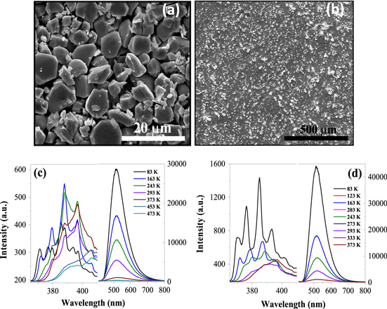
Figure 1. SEM image of (a) ZnO microcrystals and (b) ZnO microcrystals embedded in PMMA. The bright spots correspond to ZnO. Temperature dependent PL of (c) ZnO and (d) PMMA-ZnO.
Download figure:
Standard image High-resolution imageFigures 2(a) and (b) show the dependence of green to UV band intensity ratio with temperature for ZnO and PMMA-ZnO, respectively. A monotonic increase in the intensity ratio is evident as the temperature is decreased. The variation of intensity ratio with temperature suggests the possibility of ratiometric temperature sensing.
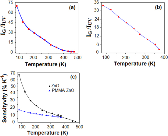
Figure 2. Temperature-dependent intensity ratio of green and UV band of (a) ZnO and (b) PMMA-ZnO, (c) the sensitivity as a function of temperature.
Download figure:
Standard image High-resolution imageOptical temperature measurement may be realized by taking the intensity ratio R of UV (IUV) and the green band (IG). The sensitivity (S) of ratiometric thermometer is defined as [6, 7]

The variation of S with temperature for ZnO and PMMA-ZnO are shown in figure 2(c). It may be noted that the sensitivity of ZnO microcrystals is 67.3 − 0.87% in the temperature range of 83–473 K, while the value ranges from 17.7 − 6.9% for PMMA-ZnO in the temperature range of 83–373 K. Because of the high stability and moderate sensitivity, the application of PMMA-ZnO in cryogenic thermometry is highly recommended.
3.2. In2O3 octahedrons in optical thermometry
Figure 3(a) shows SEM image of In2O3 octahedrons which clearly reveals average size of ∼1.5 μm. Figure 3(b) shows the typical XRD pattern of In2O3. All the peaks are indexed to the body centered cubic (bcc) In2O3 with lattice parameter 1.012 nm (JCPDS 76-0152). PL studies on In2O3 octahedrons are carried out using 355 nm laser as excitation source. Temperature dependent PL of In2O3 powder sample in 293–453 K range is shown in figure 3(c). The PL intensity decreases with increase of temperature as shown in figure 3(d). With the increase of temperature, electron–phonon interaction increases and new defect levels are created that cause the change in the peak position [23]. Furthermore, non-radiative recombination among electrons and holes increases that reduces the PL intensity with the increase of temperature [24]. It is well known that bulk In2O3 does not show any luminescence at room temperature. The nano/micro structures exhibit luminescence due to the presence of different defects such as oxygen and indium vacancy, oxygen and indium interstitials, etc in the materials [25]. Overall, the defect mediated emission is very much essential for different optical sensing applications.
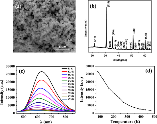
Figure 3. (a) SEM image of In2O3 octahedrons, (b) XRD pattern of In2O3, (c) temperature dependent PL spectra of In2O3 octahedron powder and (d) variation of PL intensity and peak position with temperature.
Download figure:
Standard image High-resolution image3.3. CdTe quantum dots sensitized broad-luminescent-wide band gap Ge-GeO2 for enhanced brightness
SEM image of Ge-GeO2 microcrystals is shown in figure 4(a) that clearly reveals holes with an average diameter of ∼150 nm. The synthesis and characterization of porous Ge-GeO2 has been reported in references [18, 20]. Figure 4(b) shows the PL spectra of porous Ge-GeO2 microcrystals, O-CdTe QDs and the Ge-GeO2 sensitized with O-CdTe QDs. It is interesting to note that the overall intensity in the visible region increases 10-fold by the addition of one layer of O-CdTe QDs on Ge-GeO2 pellet, while the intensity of orange luminescence corresponding to O-CdTe QDs disappears. This confirms that the visible light emission intensity of Ge-GeO2 increases when sensitized by O-CdTe QDs. Interestingly, the intensity of PL spectra increases with increasing the number of O-CdTe QDs layers. It may be noted that the intensity initially increases 40-fold and then decreases. The optical photographs of white light emission from Ge-GeO2 without and with O-CdTe layers are shown in figures 4(c) and (d), respectively. Bright white light is clearly seen as compared to the weak bluish-white light emitted only from Ge-GeO2. The blue-green-orange (white light) emission is attributed to the defects in oxides and interfacial defects between Ge-GeO2 [14, 15].
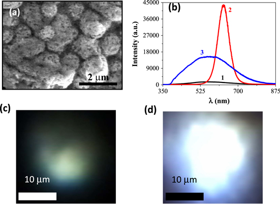
Figure 4. (a) SEM image of Ge-GeO2 microcrystal, (b) PL spectra (1–3) of Ge-GeO2 microcrystals, O-CdTe QDs and Ge-GeO2/1st layer of O-CdTe QDs, respectively, under 355 nm excitation. (c) and (d) optical images showing white light emission from Ge-GeO2 without and with O-CdTe QDs.
Download figure:
Standard image High-resolution imageForster resonance energy transfer (FRET) is one of the possible mechanisms for the enhancement in the PL intensity. In FRET, the donor molecules with higher band gap transfer the energy non-radiatively to the acceptor molecule of lower band gap [26]. The efficiency of energy transfer depends on the interparticle distance (typically <10 nm), and the overlap between donor emission and acceptor absorption spectra.
The absorption spectrum of Ge-GeO2 and the emission spectrum of CdTe QDs is shown in figure 5(a). Interestingly, the absorption spectrum of Ge-GeO2 overlaps with the emission spectra of O-CdTe QDs. As there is no signature of CdTe QDs in the PL spectra of Ge-GeO2/CdTe QDs, it is concluded that O-CdTe acts as the donor and Ge-GeO2 acts as the acceptor. When excited with 355 nm UV light, the Ge-GeO2 absorbs significantly, but the luminescence is very weak. At the same wavelength, CdTe QDs also absorb significantly and transfer the energy to Ge-GeO2. As a consequence, the luminescence of Ge-GeO2 increases and that of CdTe decreases. Overall, the experimental results support the FRET mechanism where CdTe acts as the donor and Ge-GeO2 as the acceptor.

Figure 5. (a) Overlap of absorption spectrum of Ge-GeO2 and PL spectra of O-CdTe. (b) Time resolved photoluminescence of O-CdTe QDs and Ge-GeO2/O-CdTe QDs. The excitation wavelength is 374 nm and the detection wavelength is 560 nm.
Download figure:
Standard image High-resolution image
The FRET efficiency (η) can be estimated if the luminescence lifetimes of donor with and without the acceptor are known. This is given by [26]
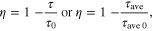
where τ, τ0 are the luminescence lifetimes of donor (CdTe) with and without the acceptor (Ge-GeO2), respectively. The average lifetime is calculated by τave = (A1τ1 + A2τ2)/(A1 + A2), where A1 and A2 are the amplitude of the decay with lifetime τ1 and τ2, respectively. The luminescence lifetime values τ and τ0 obtained from the time resolved PL spectra (figure 5(b)) are 0.25 and 1.57 ns, respectively. Based on the above equation, the FRET efficiency is estimated to be ∼84% for Ge-GeO2/O-CdTe.
4. Conclusion
We have demonstrated that the WBG green-luminescent ZnO microcrystals and In2O3 octahedrons can be used in wide range thermometry. We show that the ZnO microcrystallite powder can be used for sensing and mapping of temperature in a wide range (83–473 K) with an accuracy of 0.1 K and sensitivity better than that previously reported.
We have also shown that a weak luminescence in the visible region is seen from wide band gap materials when excited, especially with sub-band gap excitation. However, bright white light is obtained when sensitized with CdTe QDs. An unconventional Forster resonance energy transfer mechanism is proposed to understand the enhancement in bright luminescence. The efficiency of energy transfer is estimated to be ∼84% for Ge-GeO2 sensitized with orange luminescent CdTe QDs and the intensity increases 40-fold. Overall, our findings circumvent the obstacles associated with narrow band gap materials for the generation of white light.
Acknowledgments
The authors acknowledge Dr Enda McGlynn for his valuable comments and suggestions.
Footnotes
- *
Invited talk at the 7th International Workshop on Advanced Materials Science and Nanotechnology IWAMSN2014, 2–6 November, 2014, Ha Long, Vietnam.