
Abstract
In this work, TiO2 nanocrystalline thin films were obtained through evaporating Ti films by electron beam deposition (EBD) followed by thermal treatment. The results show that after annealing at 300, 400 and 450 °C for 8 h, the obtained TiO2 thin films have nanoparticle and nanorod structures of 15–30 nm diameter and 100–300 nm length. At 750 °C for 8 h, the rutile phase was formed. The incorporation of cadmium sulfide (CdS) into TiO2 nanoparticle thin films was investigated. A CdS thin film was vacuum deposited onto the pre-deposited TiO2 film by a thermal evaporation technique. The obtained TiO2 and TiO2/CdS nanocomposite films were characterized by x-ray diffraction (XRD) and a field emission scanning electron microscope (FE-SEM). The TiO2/CdS composite film was used in a photo-electrochemical (PEC) cell as a working electrode and in a platinum electrode as a counter electrode. The electrolyte solution contains 1 M KCl and 0.1 M Na2S. The results show that the cell with the TiO2/CdS composite film electrode has significantly improved photoelectric capability in comparison with that of pure TiO2 thin films, and the best thickness of the CdS thin film deposited on the ITO/TiO2 substrates is 70–140 nm.
Export citation and abstract BibTeX RIS

Content from this work may be used under the terms of the Creative Commons Attribution-NonCommercial-ShareAlike 3.0 licence. Any further distribution of this work must maintain attribution to the author(s) and the title of the work, journal citation and DOI.
1. Introduction
Titanium dioxide is a material which has attracted lots of attention due to its importance in a variety of practical applications: catalysis, energy conversion, optics, sensing, etc. TiO 2 is biologically and chemically inert, abundantly available and cheap. This material is known to exist in several forms, among the most abundant are anatase, rutile and brookite [1]. The brookite phase is stable only at very low temperatures and hence is not so useful, practically. Rutile is obtained after high temperature calcinations and its fundamental properties, such as electrical, optical and thermal, are well studied [2, 3]. In contrast, the properties of the anatase form are not so well understood. The reason could be that the anatase, which is a comparatively low temperature stable phase, has gained significance only after nanostructure materials and their synthesis started playing a major role in materials science. Therefore, considerable effort has been focused on developing simple methods for synthesis of the TiO 2 layer with the desired morphology and improved performance. In order to maintain a sustainable environment, there is high demand to produce inexpensive renewable energy sources, so the development of low production cost solar cells is of particular interest among various potential applications of TiO 2 porous layers. In optoelectronic devices, the TiO 2 porous layer serves as the route for electron transport to the anode. Therefore the morphology of Ti thin films plays a crucial role in determining the efficiency of the devices.
There are numerous reports describing the fabrication of Ti thin films using techniques such as Electron Beam Deposition (EBD) [4], doctor blading [5], magnetron sputtering [6], sol–gel processing [7], surfactant template self-assembly [8], pulsed laser deposition [9], spray pyrolysis, etc. In this work, TiO 2 nanocrystalline thin films were obtained through evaporation of Ti films by the EBD method followed by thermal treatment at 300 °C, 450 °C and 750 °C for 8 h.
Apart from its unique properties, it is well known that TiO 2 acts as a catalyst under ultraviolet excitation due to its wide bandgap (around 3.2 eV). To overcome this problem, various materials like dyes and metallic nanoparticles have been used as a sensitizer to increase the photoactivity of TiO 2 in the visible range. Combining two semiconductor particles offers an opportunity to sensitize a semiconductor material having a large bandgap and energetically low-lying conduction band by another one having a small bandgap and energetically high-lying conduction band [10]. Charge injection from one semiconductor into another can lead to efficient and longer charge separation, which is anticipated to have potential applications in photocatalysis and solar energy conversion [11]. Among the various semiconductors, CdSe, CdTe, CuInS 2, InP, etc, are used as sensitizers [10, 12–15], CdS has shown much promise as an effective sensitizer [16, 17]. CdS belongs to the II–VI group, and is typically sulfur deficient [18]. It is the most widely studied nanocrystalline semiconductor as a photoanode in photoelectrochemical cells because of its suitable bandgap, long lifetime, important optical properties, excellent stability and ease of fabrication [19–21]. However it has not been much studied in the case of Dye-sensitized Solar Cells (DSCs) [22]. In this study, CdS was used to sensitize TiO 2 nanostructures. In a TiO 2/CdS nanocomposite, CdS acts as a visible sensitizer and TiO 2, being a wide band semiconductor, is responsible for charge separation which suppresses the recombination process. Hence, the prepared TiO 2/CdS nanocomposite thin films can effectively capture the visible light and quickly transfer the photogenerated electrons into the TiO 2 conduction band, and finally, the sensitization of CdS on ITO/TiO 2 strongly ameliorates the photoelectric performance of the TiO 2/CdS nanocomposite thin films.
In this work, TiO 2 and CdS thin films have been fabricated by the EBD method combined with thermal process and thermal evaporation techniques, respectively. Compared with various techniques used for the deposition of CdS thin films in [23–27], EBD and thermal evaporation are relatively simple techniques for large scale uniform coating to produce clean, dense and strong adhesion to substrate thin films.
2. The experimental setup
A range of substrates were used for different purposes. For photo-electrochemical (PEC) cell testing, patterned ITO on glass was used. For XRD, FE-SEM samples, silicon substrates were employed. Optically transparent and electrically conductive indium tin oxide (ITO) coated glass substrate with a sheet resistance of 30 Ω per square and silicon substrates were ultrasonically cleaned in a series of organic solvents (ethanol, methanol and acetone) and deionized water. All the substrates were subsequently treated by a glow discharge technique. A 300 nm thick layer of Ti was deposited by an electron beam with 6 keV of energy at 10−5 torr pressure. The deposition rate was controlled at 0.15 nm s −1. It is well-known that thin film depositions on glass substrates are typically limited to anatase or anatase-rutile mixed phases due to the low melting point of most glasses. Therefore, the Ti coated ITO substrates were subsequently annealed at 300 °C and/or 400 °C for 8 h in air. The Ti coated silicon substrates were also annealed at 300 °C, 400 °C, 450 °C and 750 °C for 8 h in air.
The thin films of CdS were deposited by thermal evaporation under a vacuum of around 10−2 torr onto the TiO 2/ITO substrates. The deposition rate was 0.2 nm s −1. The thin film thickness in the range of 10–300 nm was measured during deposition using a conventional quartz crystal monitor. To obtain good crystallinity, the thin CdS films were annealed at 300 °C in air for 1 h [28].
The surface morphology of the samples was investigated using a Hitachi Field Emission Scanning Electron Microscopy (FE-SEM). The Ultraviolet-visible (UV-VIS) absorption spectra were measured using a Jasco UV-VIS-NIR V570 spectrometer and X-ray diffractograms were recorded on a XD-5000 diffractometer using CuKα radiation of wavelength 1.5406 Å. In photoelectronic studies, a two-electrode photoelectrochemical cell was used. The cell is composed of ITO/TiO 2 or ITO/TiO 2/CdS used as the working electrode (the working area is 0.6 cm 2) and a platinum electrode separated by an electrolyte containing 1 M KCl and 0.1 M Na 2 S. The photocurrent was measured on an Auto-Lab Potentionstat PGS-30. A halogen lamp was used as the light source.
3. Results and discussion
3.1. Morphology and structural characterization of the TiO2 thin films and the TiO2/CdS nanocomposite thin films
Figure 1 shows FE-SEM images of the annealed TiO 2 thin films (planar view) on silicon substrates at different temperatures. From the figure it is apparent that at annealing temperature of 300 °C the TiO 2 thin films have a nanoparticle structure, although conversion to TiO 2 may not be completed. The surface of the thin film is uniform and smooth with grain size less than 10 nm. The porous structure becomes visible after annealing at 400 °C. The average TiO 2 particle size was found to be less than 20 nm. The morphology and crystallinity are improved with increasing annealing temperature. The porous size is 5–10 nm and crystalline structure is anatase, which is crucial for application in solar cells [29]. It is clearly seen from the figure that at an annealing temperature of 450 °C, the TiO 2 thin film is uniform with grain size in the range of 15–30 nm.
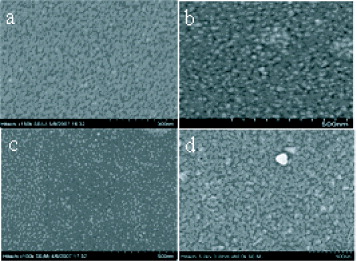
Figure 1 FE-SEM images of annealed TiO 2 thin film surfaces at (a) 300 °C, (b) 400 °C, (c) 450 °C and (d) 750 °C.
From the cross-sectional FE-SEM images of annealed TiO 2 thin films at 450 °C (figure 2(a)) and 750 °C (figure 2(b)), it can be seen that the length of the grains is from 100 to 300 nm. The TiO 2 rods are parallel to each other and perpendicular to the substrate. At an annealing temperature of 750 °C, both the planar view and cross-sectional view show the agglomeration of grains with size of about 70 nm. The rod length completely occupied the thickness of the film. Figure 3 shows the XRD pattern of the TiO 2 thin films after annealing at 450 °C (figure 3(a)) and 750 °C (figure 3(b)), respectively.

Figure 2 Cross-sectional FE-SEM images of annealed TiO 2 thin films at (a) 450 °C and (b) 750 °C.

Figure 3 XRD pattern of surfaces of TiO 2 thin films annealed at 450 °C (a) and 750 °C (b).
As can be seen from figure 3, the titanium films were completely transformed to TiO 2. In the figure, TiO 2 diffraction peaks can be assigned to the planes of the anatase and rutile phases according to the standard diffraction index. It is clear that anatase phase occurs and a small amount of rutile phase was observed at heating treatment of 450 °C. From figure 3(a) it is clearly seen that the diffraction peaks of TiO 2 annealed at 450 °C are large. It indicates that the TiO 2 films have a nanostructure. From figure 3(b), rutile peaks are found to be narrower, indicating that the TiO 2 thin film was crystallized in large grain size. The transformation from anatase phase to rutile phase was completed at 750 °C. FE-SEM images of the surface of CdS films with thickness of 70 nm and 300 nm on the ITO/TiO 2 substrates are shown in figures 4(a) and (b), respectively. As shown in the figure, homogenous CdS films with good quality were deposited onto the ITO/TiO 2 substrate and good film-to-substrate adhesion was observed. The CdS films are uniform and the surface roughness is different, in the case of films deposited with different thicknesses. Figure 4(b) shows the smooth topography of the 300 nm CdS film on the ITO/TiO 2 substrate with roughness 5–10 nm. In contrast to this, the 70 nm CdS film has a very rough surface with little aggregation of grains (figure 4(a)). Vacuum deposition by thermal evaporation can effectively improve the distribution of CdS nanoparticles around TiO 2 nanoparticles and the porosity of the thin film.

Figure 4 FE-SEM images of the 70 nm (a) and 300 nm CdS (b) on TiO 2 substrates.
The XRD pattern of ITO/TiO 2/CdS thin film shows that enhancement of the intensity of the peak at 2θ position of 26.8° corresponding to the (002) plane indicates preferential orientation in the (002) direction. This result agrees well with those of [30–32].
3.2. Absorption spectra of the TiO2/CdS nanocomposite films
Figure 5 shows the UV-VIS absorption spectra of a series of CdS thin films on the ITO/TiO 2 substrates with thickness ranging from 10 to 300 nm. As it can be seen from the figure, the TiO 2 thin film absorbs light mainly in the wavelength range from 300 to 380 nm. The absorption intensity of the TiO 2/CdS nanocomposite films increases with increase of the thickness of the CdS films. The main absorption edge for the 70 nm CdS film on the ITO/TiO 2 substrate is estimated to be about 500 nm (2.48 eV), which shifts toward the visible region compared with the pure TiO 2 thin film. This is in good agreement with Fu and coworkers [16]. In the visible region, the absorption intensity of the 200 nm CdS film on the ITO/TiO 2 substrate is appreciably higher than that of the 70, 30 and 10 nm CdS films on ITO/TiO 2 substrates, respectively. Therefore, the modification of CdS thin films for ITO/TiO 2 would effectively capture the visible light.

Figure 5 UV-VIS absorption spectra of nc-TiO 2 film and TiO 2/CdS composite films with different thickness of CdS film. Pure TiO 2 (a), CdS films of 10 nm (b), 30 nm (c), 70 nm (d) and 200 nm (e), on ITO/TiO 2 substrates, respectively.
3.3. Photoelectronic performance of the TiO2/CdS nanocomposite films
Figure 6(1) shows the photocurrent-potential behaviors of the photo-electrochemical cell with ITO/TiO 2 and ITO/TiO 2/CdS in turn under dark conditions and illumination. It is clearly seen that the photo-electrochemical cell made from films consisting only of TiO 2 has very low values for V oc and J sc , whereas on coating a thin film in CdS, both V oc and J sc increases dramatically. Figure 6(2) shows the photocurrent-potential behaviors of the photo-electrochemical cell with each of the prepared samples used as working electrodes in turn. It is clear that the coupling of CdS with TiO 2 ameliorates the photoelectric performance of the TiO 2/CdS nanocomposite films. Table 1 shows the open-circuit photovoltage (V oc ) and the short-circuit photocurrent (J sc ) of the ITO/TiO 2 and ITO/TiO 2/CdS with different thickness of CdS film. The variation in the open-circuit photovoltage (V oc ) and the short-circuit photocurrent (J sc ) is likely due to the differences in the thickness of the CdS thin films. It is clear that in the thickness range of 10–70 nm, the V oc and J sc of the film electrodes under illumination increase with increase of the thickness of the CdS thin films and approach maximum values of V oc =304 mV and J sc =35 μA (70 nm CdS film electrode). Conversely, the V oc and J sc decrease as the thickness of the CdS thin films increases in the thickness range of 70–300 nm. This can be explained as follows: the electron affinity of the CdS is higher than that of the TiO 2. Therefore, according to Anderson's model, a type-II heterojunction is formed between the CdS and TiO 2. The light from the halogen lamp generates electron–hole pairs in the CdS. The electrons from the conduction band of the CdS are quickly transferred to the conduction band of the TiO 2, as shown in figure 7. Once the electrons diffuse into the conduction band of the TiO 2, the probability of its decay is small because there is no free hole in the TiO 2 under visible excitation. As a result, the electrons accumulate in the conduction band of the TiO 2 and the holes accumulate in the valance band of the CdS. In this way, charge separation is achieved.

Figure 6 Photocurrent-potential behaviors: [Panel (1)] the ITO/TiO 2 electrode in dark conditions (a), and under illumination (b), 30 nm-CdS film on the ITO/TiO 2 substrate electrode in dark conditions (c), and under illumination (d). [Panel (2)] CdS films of 10 nm (a), 30 nm (b), 70 nm (c), 140 nm (d), 200 nm (e) and 300 nm (f), on ITO/TiO 2 substrate electrodes under illumination, respectively.
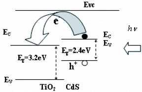
Figure 7 Schematic diagram of charge transfer at the TiO 2-CdS heterojunction interface.
Table 1. The V oc and J sc of all samples used as working electrodes in the PEC cell.
| Plain TiO 2 | 32 | 0.5 |
| 10 | 107 | 3.5 |
| 30 | 143 | 11.5 |
| 70 | 304 | 35 |
| 140 | 241 | 16 |
| 200 | 79 | 3.6 |
| 300 | 72 | 1.2 |
In photo-electrochemical measurement, in order to avoid recombination, the photogenerated holes must reach the counter electrode along continuous paths without recombining with electrons. Simultaneously, the generated photoelectrons quickly transport to the counter electrode via the external circuit. Finally, the electron cycle is ended via the redox couple in the electrolyte [16]. It is clearly seen that the coupling of TiO 2 with CdS can significantly enhance the separation of electron and hole.
However, as discussed above, the amounts of V oc and J sc of the TiO 2/CdS nanocomposite electrodes depend on the thickness of the CdS thin films deposited on the ITO/TiO 2 substrates. It is well known that light absorption with suitable wavelength results in the creation of a bound electron-hole pair, a so-called exciton.
Mobile charge carriers are generated when the electron and hole of an exciton at the interface between the TiO 2 thin film and CdS thin film are separated. Only those excitons created within a diffusion length from the charge separation region can effectively generate charge carriers. This means that only a thin slab having a suitable thickness around the interface is contributing to the current. Increasing the thickness of CdS thin films will increase the light absorption leading to greater exciton generation, as shown in figure 5, but not the charge separation and thus efficiency of the photoelectrochemical cell, for example the 200 and 300 nm CdS films on ITO/TiO 2 electrodes discussed above have the smallest values of V oc and J sc . Moreover, increase of the thickness of CdS thin films would take a longer time for the electrons to reach the interface. Therefore, the probability of recombination or trapping of the generated holes would be higher, causing the photocurrent to decrease. In contrast, for the CdS films under 70 nm, decrease of the thickness will decrease the values of V oc and j sc due to lower absorption of the CdS films. Hence, the 70 nm CdS thin film seems to be a better candidate for a photovoltaic solar cell. Qualitatively, the main reason is that the thickness might be suitable for light generated electrons and holes to travel over a shorter path and thus recombination losses are greatly reduced. Therefore, an enhanced charge transport route is desirable to achieve efficient electron conduction. In addition, the rough surface of the 70 nm CdS thin film, as shown in figure 4(a), can lead to an increased contact area to the electrolyte, which might give rise to increase of the electrical conductivity.
4. Conclusion
TiO 2 thin films have been successfully prepared by an EBD method combined with thermal process. At an annealing temperature of 300 °C, the TiO 2 thin film has a nanoparticle structure with grain size around 10 nm. The porous structure appeared after annealing at 400 °C with particle size less than 20 nm. At an annealing temperature of 450 °C, the TiO 2 thin film is uniform with grain size in the range of 15–30 nm; the length of grains is from 100 to 300 nm. The TiO 2 rods are parallel to each other and perpendicular to the substrate. At an annealing temperature of 750 °C, the TiO 2 thin film had agglomeration of grains with size of about 70 nm in diameter. TiO 2/CdS nanocomposite films have been successfully fabricated by a thermal evaporation technique. The photoelectrochemical performance of the prepared TiO 2/CdS nanocomposite thin films is superior to that of the ITO/TiO 2 film. It would mean that TiO 2 microporous structures sensitized by CdS thin films can be used for fabricating high efficiency photovoltaic devices. The best thickness of the CdS thin film deposited on ITO/TiO 2 substrates is 70–140 nm.
Acknowledgments
This work is supported in part by the National Program for Basic Researches in Natural Science of Vietnam under contract No. 103.02.82.09. A part of the work was done with the help of the Key Laboratory in Electronic Materials and Devices, Institute of Materials Science, Vietnam Academy of Science and Technology, Vietnam.