

Abstract
A 2D analytical tunnel field-effect transistor (FET) potential model with cylindrical gate (CG-TFET) based on the solution of Laplace's equation is proposed. The band-to-band tunneling (BTBT) current is derived by the help of lateral electric field and the shortest tunneling distance. However, the analysis is extended to obtain the subthreshold swing (SS) and transfer characteristics of the device. The dependency of drain current, SS and transconductance on gate voltage and shortest tunneling distance is discussed. Also, the effect of scaling the gate oxide thickness and the cylindrical body diameter on the electrical parameters of the device is analyzed.
Export citation and abstract BibTeX RIS

Original content from this work may be used under the terms of the Creative Commons Attribution 3.0 licence. Any further distribution of this work must maintain attribution to the author(s) and the title of the work, journal citation and DOI.
1. Introduction
As conventional metal oxide semiconductor field-effect transistors (MOSFETs) are downscaled to the sub-nanometre region, the close proximity between source and drain reduces the controlling capability of the gate over the channel. This leads to several problems, such as high subthreshold swing (SS), high leakage current in the OFF state (IOFF), a complex supply voltage reduction, and other short channel effects (SCEs) like threshold voltage roll-off and increased substrate bias effect [1–4]. Many researchers have adapted multigate silicon on insulator (SOI) technology, which is the potential candidate to replace bulk MOS [5–8]. However, cylindrical gate all-around MOS (GAA-MOS) provides better electrostatic control of the channel; reduces SCEs, floating body effect, and corner effects, and has better scaling option compared to trigate, double-gate and single-gate structures [9–11]. But the key challenge of GAA-MOS technology is to improve the parameters like SS and leakage current, as they lead to higher power consumption and sluggish switching characteristics [12, 13]. The SS of GAA-MOS is limited to 60 mv/decade at room temperature due to the thermionic emission of the MOS structure. The high SS of the GAA-MOSFET results in an increase in a significant amount of OFF-state current leaking in the subthreshold region, which makes the device unsuitable for low power and steeper switching applications.
Tunnel FET (TFET) is the potential solution for low power application, as it has the capability to overcome the SS limit. The carrier movement of TFET mostly depends on the nonlocal band-to-band tunnelling (BTBT) phenomena. However, TFETs can be used in faster switching applications with properly supplied voltage scaling, and the device characteristic does not depend on the temperature variation, unlike MOS [14–16]. TFET results low IOFF due to the reduced electric field at the tunnel junction in the OFF state. Therefore in recent times, many researchers have taken an interest in developing the TFET model to study the device physics for further improvement and scaling [17–19]. A number of models have been designed to compute the channel potential and tunneling current of TFET by assuming geometric tunneling paths [20, 21]. Also, a number of 2D single-gate and double-gate TFET models have been reported recently, which show the calculation of the tunneling current using the generation rate of the carrier over tunneling volume [22–26].
In this paper a p-channel cylindrical gate TFET (CG-TFET) analytical model is developed that predicts the tunneling current through a minimum tunneling path in a lateral direction. The minimum tunneling distance plays a key role for the estimation of the other electrical parameters, such as SS, ON current and transconductance. The potential distribution and electric field have also been derived for the developed model. The electrical parameters are computed by varying the Si pillar diameter from 4 to 10 nm and scaling the gate oxide thickness from 4 to 2 nm for a channel length of 50 nm.
2. Analytical model
2.1. Device structure
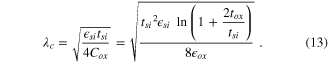
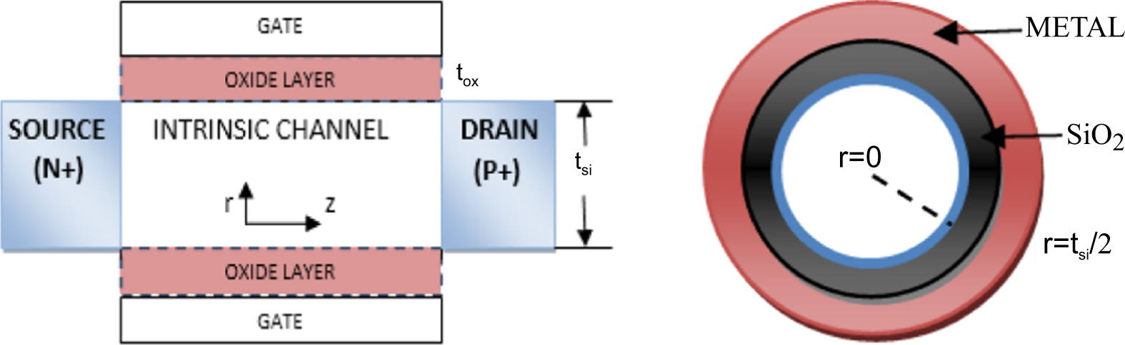
The TFET is a p-i-n diode operating in a reverse bias condition. The structural schematic diagram of the p-channel CG-TFET is shown in figure 1. The source and drain regions of the CG-TFET model are heavily doped by pentavalent impurity and trivalent impurity, respectively. However, the channel region of the device is made up of intrinsic material. For the present model, the channel is assumed to be very lightly doped of the order of 1015. The potential distribution along the channel can be estimated by solving two-dimensional Poisson's equation under parabolic approximation [10].

Figure 1. Schematic cross-sectional view and side view of p-channel CG-TFET.
Download figure:
Standard image High-resolution imageThe 2D Poisson's equation in the cylindrical coordinate is expressed as
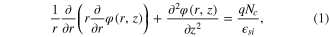
where  is the doping concentration of the thin silicon cylindrical body,
  is the electrostatic potential distribution in the intrinsic channel,
  is the dielectric permittivity of silicon and
  is the elementary electron charge. As the device body is very lightly doped (order of ∼1015), the effect of
  upon the solution of equation (1) is negligible. So equation (1) takes the form of a 2D Laplace equation as

The potential distribution along the channel is approximately defined as a parabolic equation with the boundary conditions of GAA-MOSFET [12]

The boundary conditions are essential to predict the coefficients a0, a1, a2 of the 2nd order polynomial and are finally able to find the solution of the 2D Laplace equation given by equation (2). The required boundary conditions in the intrinsic channel region are approximated as [10].
- (1)The potential at the center of the cylinder structure varies w.r.t. 'z' only

- (2)The electric field at the center of the thin silicon body is minimal and has a negligible effect on the potential distribution in the channel
- (3)The electric field at the gate oxide–channel interface is maximal and is represented as


where
Here  is the diameter of the cylindrical channel,
  is the oxide capacitance,
  is the thickness of the SiO2 layer,
  is the permittivity of the oxide layer,
  is the gate-to-source voltage and
  is the flat-band voltage.
Using the boundary conditions in equation (3), we get

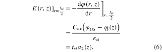
Equation (2) can be solved for the center of the cylindrical body (r = 0). Substituting equation (7) in (2) and setting r = 0, we obtain the following one-dimensional (1D) differential equation
The surface potential  is related to the center potential
  as [13]

where
Differentiating the previous equation
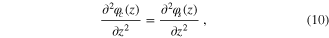
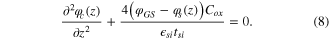
now equation (8) becomes
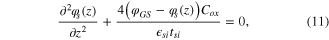

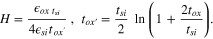
where  is known as the characteristic length of the cylindrical gate and is mathematically defined as
2.2. Surface potential distribution
The differential equation (12) can be solved by using an auxiliary equation to obtain the surface potential of the cylindrical channel as

where  and
and 
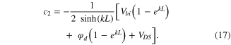
For the previous expression the coefficients c1 and c2 can be calculated by using the boundary conditions at the source and drain ends. The surface potential at the source end (z = 0) is defined as the built-in potential, which is the amount of band bending of valence band and conduction band at the source-channel interface for  Similarly, the potential at the channel-drain interface (z = zmax = L) is the sum of the built-in potential (Vbi) and drain voltage (VDS), as the channel is inverted at the drain end.
The necessary sufficient boundary conditions are [18]


Equating equation (14) using the previous boundary conditions

and
2.3. Electric field analysis
The electric field of the channel can be derived by differentiating electrostatic potential distribution w.r.t. r and z ( ).
).
The radial and lateral electric fields are expressed as
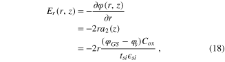
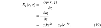
However, for a TFET model, the tunneling process is dominant in the lateral z-direction compared to the radial direction [27]. So the lateral electric field along the length of the channel is considered in the next section to calculate the tunneling current.
2.4. Tunneling phenomena
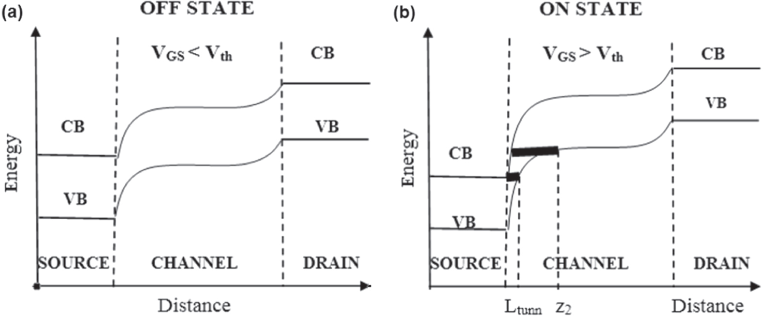
The tunneling of the charge carrier at the source end starts only when the conduction band of the source gets aligned with the valence band of the intrinsic channel region. The shortest tunneling distance (Ltunn) is the lateral distance between the source-channel interface (z = 0) and the point in the channel where the surface potential changes by an amount of unit bandgap energy per elementary charge (Eg/q). However, the shortest tunneling distance plays a crucial role in finding the amplitude of the tunneling current in the device.
The gate voltage has a significant effect on the tunneling phenomena as shown in figure 2. At low gate voltage, there is a small amount of band bending of the valence band and conduction band. So the current is negligible due to the absence of BTBT of the charge carrier. For a critical value of the gate voltage known as the threshold voltage (Vth), the conduction band of the source and the valence band of the channel are in line to each other. For VGS > Vth, the tunneling probability increases, which improves the BTBT current in the channel. The BTBT drain current increases exponentially due to the improvement in tunneling volume as depicted by the area under the solid lines in figure 2(b). Ltunn is calculated for the values of z at which the potential energy changes by EG/q. The critical threshold condition is expressed as


Figure 2. Energy band diagram of p-channel CG-TFET in (a) OFF state and (b) ON state showing shortest tunneling distance (Ltunn) with different gate bias condition.
Download figure:
Standard image High-resolution imageThe corresponding potential values for z = 0 and z = Ltunn are obtained from the defined boundary conditions

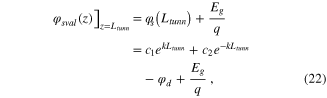
where  and
and  are the conduction potential of the source and valence potential of the channel.
The value of the shortest tunneling distance can be obtained from the critical threshold condition as
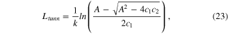
where A is the device-dependent constant and expressed as
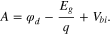
However, the shortest tunneling distance can be reduced by using low bandgap material and increasing the gate potential (VGS), which increases the tunneling volume in the channel region. The higher the tunneling volume, the greater the ON current of the device. For a constant gate voltage, the tunneling volume is not affected by drain voltage.
2.5. Drain current analysis
The drain current of the proposed model is calculated analytically by Kane's model, which uses a nonlocal BTBT approach. However, Kane's model [28] is used to find the rate of generation of carrier ( tunneling from source to drain along the channel as:
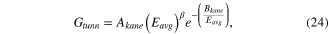
where  and
and  are tunneling-dependent parameters and the default values of
  and
and  [29].
[29].  is the material-dependent parameter and its value depends on the type of tunneling, i.e., 2.5 for the indirect tunneling and 2 for direct tunneling [29]. However, in the present analysis the value of
  is considered as 2.
  is the average electric field over the tunneling volume and is expressed as
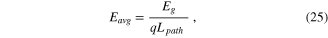
here  is the length of the BTBT tunneling path, which varies over the tunneling volume in the z-direction. From figure 2, the
  is described as the path between two lateral points z1 = Ltunn and z2.
Now the drain current can be computed with the help of the BTBT generation rate

Substituting the value of the lateral electric field and the average tunneling field from equations (19) and (25)
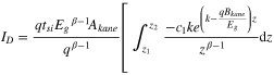
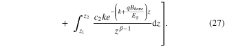
Here, the tunneling of the charge carrier takes place between two lateral points z1 = Ltunn and z2. Between the two boundaries along the z-direction, the effect of the polynomial term ( is negligible as compared to the exponential term
  So the drain current is obtained by integrating equation (27) over the tunneling interval and neglecting the polynomial term; thus, we get

where  and
and  are expressed as
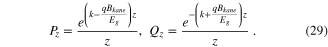
As  it is noted that the exponential coefficient
  and
and  In the present model, the current analysis is carried out by neglecting the minimal effects of
  and
and  and instead using the shortest tunneling distance (
 ).
).
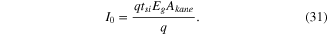
where I0 is the dc current that only depends on constant parameters and is defined as
2.6. Subthreshold swing (SS)
SS is a feature of a MOSFET's current–voltage characteristic in the sub-threshold region (VGS < Vth) and is defined as the slope of logarithmic drain current w.r.t. gate voltage at a constant drain voltage. The inverse of this slope is usually referred to as SS in mV/decade

The optimum value of the SS of a conventional MOSFET is 60 mV/decade at room temperature (300 K). It is always desirable to have a small SS, as it improves the  ratio by reducing the leakage of the OFF state current. Also the low SS or steep subthreshold slope of a device indicates the faster switching behavior, i.e., faster transition between OFF state and ON state. SS can be computed by substituting the value of ID in equation (32)
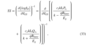

where
It is noted that the model offers an SS of 26 ∼ 40 mV/decade compared to the GAA-MOS limit of 60 mV/decade over a wide range of gate voltages, as shown in table 1. This leads to a reasonable amount of improvement in 
Table 1. Subthreshold slope for CG-TFET in subthreshold region.
| Drain voltage (V) | Gate oxide thickness (nm) | Si pillar diameter (nm) | Subthreshold slope (mV/decade) |
|---|---|---|---|
| –1 | 2 | 10 | 27 |
| –1 | 3 | 10 | 44 |
| –1 | 4 | 10 | 56 |
| –1 | 4 | 8 | 46 |
| –1 | 4 | 6 | 38 |
2.7. Transconductance
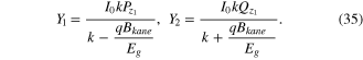
Transconductance ( is the transfer characteristics of the device and is calculated by differentiating equation (30) w.r.t. VGS at constant VDS.
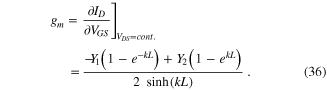
As gate oxide thickness reduces, the effective gate control over the channel improves and conversely increases transconductance of CG-TFET as depicted in figures 12 and 13.
3. Results and discussion
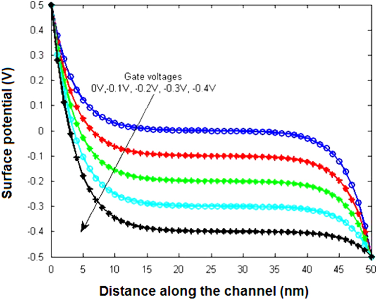
Figure 3 illustrates the surface potential profile in the cylindrical p-TFET for different gate voltages. The potential is pinned to Vbi and Vbi + VDS at the source and drain end as per the boundary conditions defined in equation (15). As the gate voltage increases for constant drain voltage, the potential in the intrinsic channel region improves. However, we get a constant surface potential at the middle of the channel. This is due to the saturating effect of gate control over the channel. Also the variation of surface potential near the tunneling junction is less because the charge carriers vary less. The slope of the potential distribution decreases along the channel from source to drain end.

Figure 3. Surface potential distribution of p-channel CG-TFET for 50 nm channel length and −1 V drain voltage at different gate voltages.
Download figure:
Standard image High-resolution imageFigure 4 shows the behavior of lateral and radial electric fields for different gate voltages for a 50 nm channel. It is clearly seen from the figure that the electric field varies non-linearly at the source and drain ends. The variation of the field arises at the source-channel interface because of the tunneling phenomena, and the same results at the drain interface are due to the influence of the drain potential. The constant potential in the middle of the cylindrical body gives rise to a constant electric field in both directions. The radial and lateral field reaches zero at the middle of the channel due to zero slope potential.
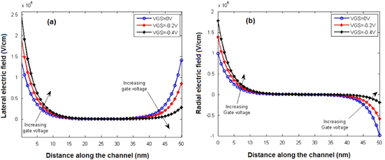
Figure 4. Lateral electric field (a) and radial electric field; (b) distribution of p-channel CG-TFET for 50 nm channel length and −1 V drain voltage at different gate voltages.
Download figure:
Standard image High-resolution imageThe shortest tunneling distance as a function of gate and drain voltage is shown in figure 5. As the gate voltage increases beyond the threshold level, the tunneling of charge carriers from source to channel improves. Thus, Ltunn is achieved at a very small lateral distance from the source end as depicted in figure 5. But Ltunn does not change significantly due to variation of the drain voltage (figure 5(b)). However, the drain output voltage plays an important role in deciding the tunneling volume. For higher VGS, small Ltunn is achieved, which increases the tunneling volume based on drain voltage.
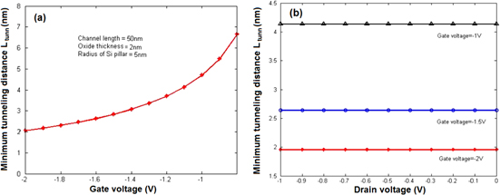
Figure 5. Shortest tunneling distance (Ltunn) variation with (a) gate voltages at constant drain voltage and (b) drain voltage at different gate voltages.
Download figure:
Standard image High-resolution imageAs the gate voltage increases beyond the threshold, Ltunn reduces for a fixed gate oxide thickness and cylindrical body diameter. However, as the gate oxide thickness (tox) is scaled from 4 to 2 nm for radii 5 nm, the tunneling is achieved faster due to reduction of Ltunn as depicted in figure 6(a), which improves the device performance by increasing BTBT current. So at low gate oxide thickness, the gate has a greater impact on the channel and threshold achieved at a low VGS, enabling flow of charge carriers. Similarly, figure 6(b) shows the variation of Ltunn versus VGS for different Si body diameters. When the radius of the cylindrical body goes on reducing for constant tox, the effect of the gate over the cylindrical body is dominant compared to the drain and thereby reduces Ltunn marginally. However, it is clearly evident from figure 6 that the effect of tox scaling has a greater impact compared to Si pillar diameter scaling on TFET ON current performance.

Figure 6. Impact of (a) gate oxide scaling and (b) cylindrical body thickness scaling on shortest tunneling distance (Ltunn) versus gate voltages.
Download figure:
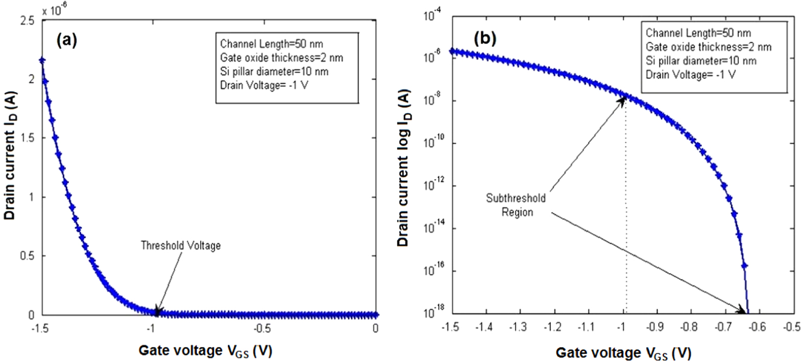
Standard image High-resolution imageFigures 7 and 8 show the graph of ID-VGSand ID-VDS characteristics for CG-TFET. Here it is observed that the tunnel drain current improves exponentially at the ON condition (VGS > Vth) due to the dominant tunneling process. Figure 7(b) displays the logarithmic ON current that helps to find the OFF current and SS in the sub-threshold region (VGS < Vth). Table 1 displays the measured SS in the sub-threshold region for different tox and tsi. However, at higher gate voltages, the tunneling volume gradually saturates and leads to the saturating drain current.
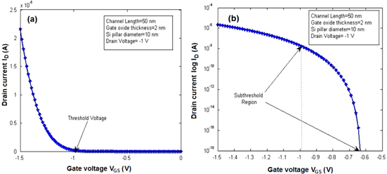
Figure 7. ID-VGS characteristics for the proposed p-channel CG-TFET. The drain current is plotted on (a) linear scale and (b) logarithmic scale.
Download figure:
Standard image High-resolution image
Figure 8. ID-VDS characteristics for p-channel CG-TFET. The drain current is plotted on (a) linear scale and (b) logarithmic scale.
Download figure:
Standard image High-resolution imageFigure 9 displays the effect of gate oxide thickness on the drain current analysis of the model. It is clearly seen that for small gate oxide thickness, the tunneling current is higher as depicted in figure 9(a). This is due to the small value of the minimum tunneling distance that leads to a large tunneling volume and maximum ON current. For a constant value of gate oxide thickness, the tunneling current increases sharply with small Ltunn as in figure 9(b). However, as the oxide thickness is scaled from 4 nm to 2 nm, the minimum tunneling distance (Ltunn) is achieved early, at a 3 nm distance from the source end, which improves the non-local BTBT tunneling of charge carriers.
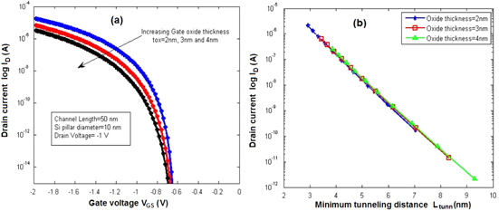
Figure 9. Impact of gate oxide scaling on drain current ID versus VGS (a) and versus Ltunn (b).
Download figure:
Standard image High-resolution imageThe effect of cylindrical body thickness on drain current analysis of the model w.r.t. gate voltage and shortest tunneling distance, respectively, is depicted in figure 10. The BTBT tunneling takes place faster for small radii and conversely improves the tunneling current. But in the sub-threshold region (VGS < Vth), the effect of the variation of the cylindrical body diameter is insignificant on drain current due to the absence of BTBT tunneling of carriers. However, the present TFET model produces a steep SS in the range of 27–56 mv/decade as presented in table 1. SS can also be calculated for different gate voltages in the sub-threshold region as shown in figure 11.
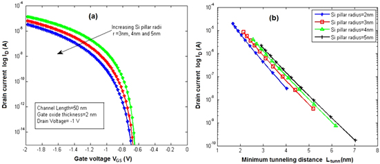
Figure 10. Impact of cylinder diameter scaling on drain current ID versus VGS (a) and versus Ltunn (b).
Download figure:
Standard image High-resolution image
Figure 11. Variation of sub-threshold slope with gate voltage in sub-threshold region.
Download figure:
Standard image High-resolution imageFigure 12 shows the transconductance as a function of gate voltage at a constant drain voltage of −1 V. It is clearly evident from figure 12(a) that for a particular value of oxide thickness, the transconductance improves above the threshold value of the gate bias. This is due to the fact that for VGS > Vth, the increased tunneling current saturates the mobile charge carriers and decreases the resistance and results in an increment of transconductance beyond the threshold voltage. Figure 12(b) shows the logarithmic values of transconductance for different gate oxide thickness. However, the transconductance improves further by reducing the gate oxide thickness due to low resistance and small tunneling distance. Further, figure 13(a) displays the relationship between transconductance and Ltunn, which concludes that 2 nm oxide thickness produces high transconductance compared to 4 nm, as Ltunn is achieved earlier.
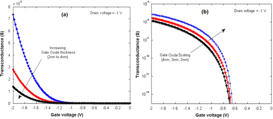
Figure 12. Variation of transconductance as a function of gate voltage for different gate oxide thicknesses in CG-TFET (a) linear scale and (b) logarithmic scale.
Download figure:
Standard image High-resolution image
Figure 13. Variation of transconductance as a function of shortest tunneling distance in CG-TFET (a) gate oxide scaling and (b) Si pillar diameter.
Download figure:
Standard image High-resolution image
The relationship between transconductance and Ltunn for different diameters of the cylindrical body is plotted in figure 13(b). The transconductance of the device enhances with the reduction of the cylinder radii, as the tunneling current increases for a large tunneling volume.
CG-TFET produces low SS (SS < 60 mV/decade), better gate oxide thickness scalability and cylindrical body diameter scalability. Therefore, this model can be a potential candidate for ultra-low-power CMOS applications in the near future.
4. Conclusion
In this paper, an accurate, physics-based model for p-channel CG-TFET is developed. The tunneling current in the proposed device is derived using a generalized Kane's model and expressed as a function of gate voltage. The drain current shows the impact of shortest tunneling distance, gate oxide thickness and cylindrical body diameter. Also, the improved SS that resulted for the present model (27 ∼ 56 mV/decade) allows the device to be a promising candidate for low-power and high-speed applications.