


Abstract
In this paper a new conical surrounding gate metal-oxide-semiconductor field effect transistor (MOSFET) with triple-material gate has been proposed and verified using TCAD device simulator from Synopsis. The electrostatic performance of conical model with different tapering ratios is extensively investigated and compared with that of cylindrical model (tapering ratio TR = 1). The present model exhibits improved electrostatic behavior for an optimized tapering ratio of 0.98 as compared to the conventional cylindrical model. The results reveal that the triple-material conical model provides better ON current performance, transconductance and reduced threshold voltage. On the contrary the single-material conical model exhibits maximum  /
/ ratio, minimum OFF current and reduced subthreshold swing (SS) in comparison to other models. Thus, the conical model with optimized tapering ratio can be a possible replacement of cylindrical model for low-power and high speed application.
Export citation and abstract BibTeX RIS

Original content from this work may be used under the terms of the Creative Commons Attribution 3.0 licence. Any further distribution of this work must maintain attribution to the author(s) and the title of the work, journal citation and DOI.
1. Introduction
In the present state of affairs, gate-all-around (GAA) technology has become a strong entrant in the nanoscience and nanotechnology sphere, with its improvement in drain current and suppression of short channel effects offering great promise. Cylindrical surrounded gate (CSG) metal-oxide-semiconductor field effect transistor (MOSFET) is one of the emerging members of GAA family which is the most probable victor for present complementary metal–oxide–semiconductor (CMOS) technology [1–6]. Every day this unique device is producing considerable surprises in the technologically imperative and application-rich areas. It is the preeminent solution to overcome the scaling limitations of planar devices and to achieve high packing density for future circuit analysis [7–11]. As the dimensions of devices shrunk down, the short distance between the source and drain reduces the gate controllability by disturbing the potential distribution and hence the flow of electrons in the channel. Short channel devices exhibit more sub-threshold leakage current and high sub-threshold swing [12–17]. The present technology demands reduction of threshold voltage for high speed applications. Continuous scaling and improvement in device design are still going on to improve device performance. Modification in device geometry from its conventional shape may improve device performance and reduce its limitation.
In this paper a conical GAA architecture is designed with single-gate material (SM), double-gate material (DM) and triple-gate material (TM), respectively. Here the drain side is tapered as compared to the source side and thus resembles the shape of a cone. The electrostatic characteristics of conical surrounding gate MOSFET are shown with different tapering ratio to check its capability. However the results obtained are compared with single-material, double-material and triple-material cylindrical gate MOSFET.
2. Device structure and simulation
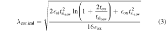
Figure 1 illustrates the simulated 3D geometry of a SM conical surrounding gate MOSFET and figure 2 shows the schematic cross-sectional view of n-channel SM, DM and TM conical surrounding gate MOSFET. For the present model the channel length is considered as 60 nm with source/drain extension of 20 nm. The source and drain are uniformly doped with pentavalent impurity having concentration of NS = ND = 1020 cm−3. The channel region is lightly doped with trivalent impurity of the order of 1016 cm−3. The model is having conical gate of diameter 10 nm at source and tapered towards drain (8 nm–9.8 nm). The conical gate thickness and oxide thickness (tox) of SiO2 layer is considered as 8 nm and 2 nm respectively. The work-functions of gate metals chosen are 4.8 eV, 4.7 eV and 4.6 eV respectively. The drain terminal of the present model is tapered as compared to the source end. The natural length of the cylindrical body structure is given by
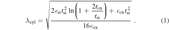
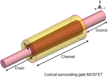
Figure 1. Simulated 3D geometry of conical surrounding gate MOSFET.
Download figure:
Standard image High-resolution image
Figure 2. Schematic cross-sectional view of n-channel SM, DM and TM conical surrounding gate MOSFET.
Download figure:
Standard image High-resolution imageHere 
 represent the permittivity and thickness of silicon,
  the permitivity of SiO2. The tapering ratio at both drain and source ends is the same as that for the conventional cylindrical structure which accounts for the uniform silicon thickness throughout the device. On the contrary the tapering ratio for the conical structure is the combination of different small cylinders with variable silicon thickness. If
  is the thickness for the cylinder with larger diameter and
  is the thickness of the cylinder having smaller diameter then

Here the natural length of the present model is expressed as
The simulation work is carried out using the 3D device simulator Sentaurus from Synopsis Inc. [18]. The electrostatic behavior of the conical model has been investigated using conventional drift-diffusion transport model. The current densities for electrons and holes are represented as [10]
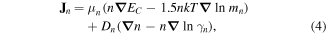
Here J represents current density, μ is the mobility, γ is the Fermi statistics constants, m represents the effective mass and D is the diffusion constant. Similarly EC and EV are the conduction band and valence band energies, respectively. However different models such as Shockley–Read–Hall (SRH) generation model and avalanche generation model are required to analyze the generation–recombination process [19]. Here the carrier mobility model considers the effect of doping concentration, velocity saturation, and transverse electric field. The old Slotboom model is used for bandgap narrowing which determines the intrinsic carrier concentration required for the model [20, 21].
3. Results and discussion
Figure 3 shows the variations in surface potential of SM, DM and TM conical surrounding gate MOSFETs. The surface potential is also compared to that of conventional cylindrical structures. It is evident that the surface potential profile for all three structures is shifted upward for conical surrounding gate MOSFET towards the tapering end due to the narrowing of silicon film.

Figure 3. Surface potential as a function of distance along the channel for SM, DM, TM cylindrical and conical surrounding gate MOSFETs.
Download figure:
Standard image High-resolution imageFigure 4 shows the variations in electric field of the present model along the channel. The conical model provides a sudden increase in the electric field at the interface of gate materials alike the cylindrical model. This is the result of work-function variation at the interface. The peak electric field at the tapering edge is minimum for triple material and maximum for single material gate due to the step change in surface potential. The field reduces as we move towards the drain end. This decrease in electric field determines the durability and stability of the device because of reduction of hot carriers.

Figure 4. Electric field variation versus distance along the channel for SM, DM, TM cylindrical and conical surrounding gate MOSFETs.
Download figure:
Standard image High-resolution imageThe different trends for a number of figures of merits have been analyzed due to the variation in the tapering ratio. From figure 5, it is observed that the conical device gives more drain current as compared to the conventional cylindrical device. However the drain current of single material gate structure is lower compared to other two conical structures. Similar analysis was performed by taking different tapering ratios (0.8–0.98) of conical structures as shown in figure 6. The tapering ratio of 0.98 gives maximum on current compared to other models. Also it has been observed that drain current of triple-material (TM) > double-material (DM) > single-material (SM) gate [22–25]. This increase in drain current for conical model is due to pumping effect, which arises because of tapering of the channel towards drain end. Tapering of the channel creates a strong electric field and thus increases the mobility of the electron. Further reduction in tapering ratio reduces the silicon thickness which adversely affects the mobility and current conduction of the device.

Figure 5. Drain current as a function of gate voltage for SM, DM, TM cylindrical and conical surrounding gate MOSFETs.
Download figure:
Standard image High-resolution image
Figure 6. On current as a function of tapering ratio (TR) for SM, DM, TM cylindrical and conical surrounding gate MOSFETs.
Download figure:
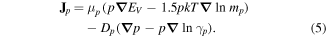
Standard image High-resolution imageTransconductance determines the gain of the device. The increase in mobility leads to an increase in transconductance. Figures 7(a) and (b) illustrate the variation of transconductance versus tapering ratio (TR) and gate voltage. It is observed that conical structure provides more transconductance with a tapering ratio of 0.98 as compared to cylindrical structure (TR = 1). The use of multi-gate technology enhances further the transconductance of the conical structure.
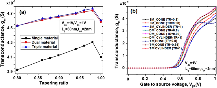
Figure 7. Transconductance as a function of (a) tapering ratio and (b) gate voltage for SM, DM, TM cylindrical and conical surrounding gate MOSFETs.
Download figure:
Standard image High-resolution imageDifferent conical and cylindrical devices were simulated and the V-I characteristics are shown in figure 8. The results show that the conical structure provides better drain current compared to cylindrical structures. Similar analysis was performed for smaller and larger tapering ratio of the conical structures and found to be maximum at a tapering ratio of 0.98 of TM-CONE. In case of TM, presence of two screening gate and one control gate create two steps in the potential profile due to difference in work function of the metals. This results increase in lateral electric field by permitting the carriers to move faster. Hence the drain current is improved.
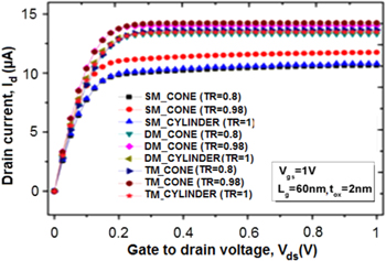
Figure 8. Drain current versus drain voltage for SM, DM, TM cylindrical and conical surrounding gate MOSFETs.
Download figure:
Standard image High-resolution imageOff current (Ioff) plays a vital role in device operation as well as its stability. For Vgs < Vth, the MOSFET operates in off-state and an undesirable leakage current flows through the channel known as off current. It is necessary to keep Ioff very small in order to reduce the static power dissipation while the device is in idle state. From figure 9 it can be concluded that conical device gives lower off state leakage current as compared to the cylindrical structure. However for dual and triple materials, the reduction in off current with tapering ratio is more prominent as compared to single material structures. The reason behind the prominence of Off current in case dual and triple material structures is due to the screening gate effect which protects the device from leakage current during the device ideal state. For dual material this leakage is controlled by single screening gate while for triple material there are two screening gates which prevent the device from barrier lowering.

Figure 9. Off current as a function of tapering ratio for SM, DM, TM cylindrical and conical surrounding gate MOSFETs.
Download figure:
Standard image High-resolution imageFor long channel devices, the existence of Ioff is not significant. However this also reduces the On current and affects speed of the circuit. So the conflict between Ion and Ioff should be minimum for the development of a standard device. Therefore the design of a device should be in such a way that, it must deliver a high Ion/Ioff ratio. From the figure 10, it is observed that conical structure exhibits higher Ion/Ioff ratio, which can make it a competitor in GAA family. Use of multi-gate technology reduces Ion/Ioff ratio as Ioff is significant as compared to single gate material.
Figure 10. Ion/Ioff ratio w.r.t tapering ratio for SM, DM, TM cylindrical and conical surrounding gate MOSFETs.
Download figure:
Standard image High-resolution imageFigure 11 shows the variation of threshold voltage versus tapering ratio. It is evident that the conical structures exhibit lower threshold voltage compared to cylindrical structure (TR = 1) for single, dual and triple material. However with variation in tapering ratio, the threshold voltage gets shifted due to shifting in surface potential and increase in transconductance. The threshold voltage is minimum for triple-material gate structure.

Figure 11. Threshold voltage as a function of tapering ratio for SM, DM, TM cylindrical and conical surrounding gate MOSFETs.
Download figure:
Standard image High-resolution imageSubthreshold slope is an important parameter during the short-channel immunity calculation of a device. In order to get high Ion/Ioff ratio, the sub threshold slope should be low. From the figure 12, the conical structure exhibits lower subthreshold slope compared to cylindrical structures at an optimized tapering ratio of 0.98.

Figure 12. Subthreshold slope as a function of tapering ratio for SM, DM, TM cylindrical and conical surrounding gate MOSFETs.
Download figure:
Standard image High-resolution image
4. Conclusion
In this paper a triple material gate conical model with different tapering ratios has been developed. The effect of tapering ratio on various electrical parameters such as drain current, surface potential, threshold voltage and subthreshold swing (SS) have been analyzed. However the results of the triple-material conical model are compared to those of the double material, single material and conventional cylindrical model. It can be evident from the results that triplet-material conical model provides higher drain current and minimum threshold voltage, whereas single-material conical model exhibits maximum  /
/ ratio and least SS for an optimized tapering ratio of 0.98. The model results are verified using a 3D device simulator from Synopsis.