

Abstract
This study optimizes Si1−xGex based double gate tunnel field effect transistor (TFET) for their high ON current (Ion) and lesser sub-threshold swing and compares Si and Si1−xGex based single material double gate (SMDG) and dual material double gate (DMDG) TFETs. This study also measures the two RF performance metrics, unity gain cut-off frequency (ft) and maximum oscillation frequency (fmax) by varying the structural parameters, gate length, gate oxide thickness, channel thickness and underlap. Compared to single material gate devices, dual material gate devices give higher Ion without compromising the leakage current for both Si and Si1−xGex based TFETs. Si1−xGex based TFETs offers higher ft and fmax compared to that of Si TFETs for all the structural parameter variations considered in this study. DMDG TFETs exhibit higher ft with respect to SMDG TFETs. SMDG TFETs offers more fmax compared to DMDG TFETs due to the smaller values of output conductance.
Export citation and abstract BibTeX RIS

Original content from this work may be used under the terms of the Creative Commons Attribution 3.0 licence. Any further distribution of this work must maintain attribution to the author(s) and the title of the work, journal citation and DOI.
1. Introduction
To meet the scaling demands, many novel devices have been reported with different working principles. Tunnel field effect transistors (TFETs) is one of the promising devices to replace MOSFET because of its sub-threshold swing (SS) limit of 60 mV dec–1, low OFF-state leakage current and low threshold voltage [1–3]. TFET is basically a reverse biased P–I–N junction diode which works on the principle of quantum mechanical band-to-band tunneling (BTBT) mechanism.
Double gate (DG) TFETs shows improved characteristics in terms of higher drive current and less threshold voltage roll-off compared to single gate TFET [4–6]. A dual material double gate (DMDG) TFET was proposed by using two different gate electrode work functions to improve the overall performance of the device [7, 8]. Since silicon (Si) based DG TFETs suffers from lesser ON-state current, this can be further improved by using lower band gap material like silicon–germanium (SiGe) for the entire region [9], or in the source channel region [10], or in the source only [11–13]. By optimizing mole fraction (x) presented in Si1−xGex, TFET exhibited higher performance with low SS [14, 15].
In this paper the optimization of Si1−xGex based DG TFET is performed to obtain a higher ON state current with lesser SS. To improve the RF metrics, unity gain cut-off frequency (ft) and maximum oscillation frequency (fmax), the structural parameters are varied for Si and Si1−xGex based single material double gate (SMDG) and DMDG TFETs. Section 2 describes the device structures of Si and Si1−xGex DG TFET along with the simulation methodology. The results are discussed in section 3. Finally section 4 provides the conclusion.
2. Device structure and simulation methodology
TCAD simulator from Synopsys is used to perform the simulations [16]. Figure 1 depicts the 2D structure of Si and Si1−xGex based n-type SMDG TFET. The schematic diagram of DG TFET is shown in figure 2 which shows various parameters of the device. The device has the gate length (Lg) of 50 nm, a channel thickness (Tch) of 10 nm, underlap (Lun) of 3 nm and gate oxide thickness (Tox) of 3 nm. The source is doped with p+ type material while the drain is doped with n+ type material. The drain doping (Nd = 5 × 1018 cm−3) is lower than source doping (Ns = 1 × 1020 cm−3) to suppress the ambipolar effect [17]. The channel has an intrinsic concentration of 1 × 1017 cm−3. The gate electrode work function for SMDG TFET is 4.5 eV.

Figure 1. Simulated structure of SMDG TFET: (a) Si based SMDG TFET (with and without doping) and (b) Si1−xGex based SMDG TFET (doping not shown).
Download figure:
Standard image High-resolution image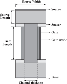
Figure 2. Schematic structure of DG TFET.
Download figure:
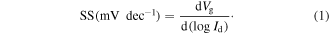
Standard image High-resolution imageThe device simulator includes appropriate models for doping dependence mobility, effects of high and normal electric fields on mobility and velocity saturation. A non-local Hurkx BTBT model is used along with Fermi–Dirac statistics and Shockley–Read–Hall recombination model. Supply voltage used in this study is 1 V and the gate voltage is 1.8 V. To operate the device, the source is grounded and the positive voltage is applied at the drain. The gate voltage (Vg) controls the tunneling by modulating the carrier concentration in the channel region. The SS of the device is defined as the change in gate voltage in order to create one decade increase in the output current. It can be expressed as
The TFET ON currents are based on BTBT mechanism. The BTB tunneling probability can be analytically calculated using Wentzel–Kramers–Brillouin (WKB) approximation method. The result of WKB approximation derived in [18] can be described by [19]

where m* is the effective carrier mass, Eg is the bandgap, e is the electron charge, ΔΦ is the energy range over which the tunneling can take place,  is the Planck's constant and Λ is the spatial extent of the transition at source-channel interface. Λ can be defined by

where tox, tSi, εox, and εSi are the oxide and silicon-film thicknesses and dielectric constants, respectively. Equation (1) shows that the tunneling current can be increased by increasing electric field along the channel (proportional to (ΔΦ + Eg)/Λ). One of the approaches to improve the performance of the device is to decrease the bandgap of the material. The amount of Ge content (x) for the Si1−xGex based DG TFETs improves the ON state current [14, 20]. Figure 3 represents the Id–Vg characteristics of Si1−xGex based SMDG TFET with Ge mole fraction (x) which is varied from 0 to 0.4. It is observed that the maximum Ion of 23 μA and lesser SS of 32 mV decade–1 are obtained for x = 0.4. This is because of the lower band gap energy for germanium over silicon. Since lesser SS is obtained for a higher Ion, mole fraction of x = 0.4 is used for SiGe devices.
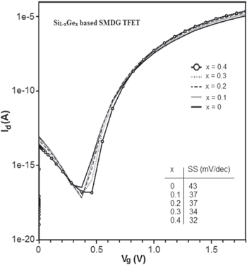
Figure 3. Id–Vg characteristics of Si1−xGex based SMDG TFET for various mole fractions ranging from x = 0 to x = 0.4.
Download figure:
Standard image High-resolution imageFigure 4 shows the energy band diagram for Si and Si0.6Ge0.4 based DG TFETs. In the OFF-state (Vg = 0 V), the tunneling barrier width is extremely large enough to give a very small leakage current. When the gate voltage is increased (Vg = 1.8 V), the conduction bands in the intrinsic region are pulled downwards and the tunneling barrier width is reduced allowing electrons move from the source to the channel region [9–11].
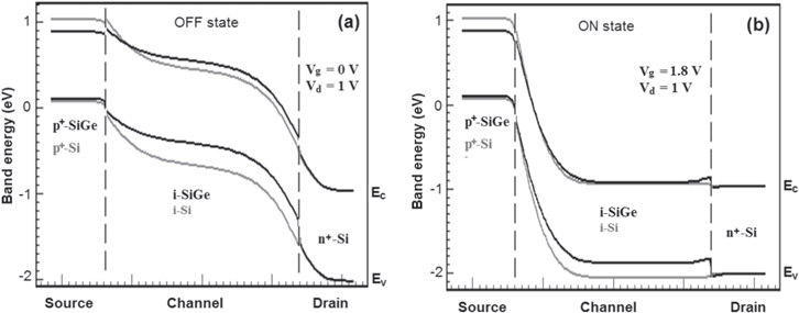
Figure 4. Energy band diagrams for Si and Si0.6Ge0.4 based DGTFETs: (a) OFF state and (b) ON state.
Download figure:
Standard image High-resolution imageThe DMDG TFETs have similar dimensions of SMDG TFETs. To get a fair comparison between Si and Si0.6Ge0.4 based SMDG and DMDG TFETs, leakage current (Ioff) of all of these devices are matched to 82.7 fA. Id–Vg characteristics of SMDG and DMDG of Si and Si0.6Ge0.4 based TFETs are extracted and plotted in figure 5. It can be seen from the graph that, compared to SMDG, DMDG offers more Ion for both Si and Si0.6Ge0.4 based TFETs. This is due to the higher tunneling probability near the source end which enhances Ion significantly [21–23]. Because of the property of double material gate and also due to the tunneling phenomenon, DMDG TFET shows the lower threshold voltage than SMDG TFET [20].
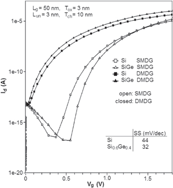
Figure 5. Id–Vg characteristics of Si and Si0.6Ge0.4 based SMDG and DMDG TFETs with Ioff = 82.7 fA.
Download figure:
Standard image High-resolution imageFigure 6 shows the plot of electron barrier tunneling with respect to distance along the channel for Si and Si0.6Ge0.4 based SMDG and DMDG TFETs. The physical significance of this plot represents the rate at which electrons are generated due to tunneling. It can be observed that DMDG TFETs show higher tunneling rate of electrons compared to that of SMDG. Comparatively Si0.6Ge0.4 offers more electron tunneling over Si based TFETs.
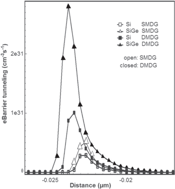
Figure 6. eBarrier tunneling for Si and Si0.6Ge0.4 based SMDG and DMDG TFETs.
Download figure:
Standard image High-resolution imageFor the devices mentioned above, the structural parameters considered here are the gate length, gate oxide thickness, channel thickness and underlap. The important RF parameters, ft and fmax are extracted by performing AC simulations. ft is defined as the frequency where current gain becomes unity and in terms of device parameters it can be expressed as

where gm is the transconductance and Cgg is the combination of gate-source capacitance (Cgs) and gate-drain capacitance (Cgd). fmax is defined as the frequency at which power gain drops to unity and can be expressed as

where Rg is the gate resistance and gds is the output conductance.
3. Results and discussion
As mentioned earlier, the gate length, gate oxide thickness, channel thickness and underlap are varied as shown in table 1. The RF parameters, ft and fmax are extracted for all these devices.
Table 1. Range of values for the structural parameters considered.
| Parameters | Range of values (nm) |
|---|---|
| Gate length (Lg) | 40–60 |
| Gate oxide thickness (Tox) | 1–5 |
| Channel thickness (Tch) | 5–15 |
| Underlap (Lun) | 1–10 |
3.1. Variation in gate length
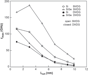
Figure 7 shows the variations of ft versus Lg. It can be observed that ft decreases with increasing gate length. Though ft is determined by both gm and Cgg, ft decreases because of gm degradation for higher gate lengths [24]. Since Si0.6Ge0.4 based TFETs offers more gm comparatively, they exhibits higher cut-off frequencies.

Figure 7. The unity gain cut-off frequency ft versus gate length Lg.
Download figure:
Standard image High-resolution imageFigure 8 shows the variations of fmax versus Lg. Compared to ft, fmax shows higher value because of the inversion layer formed in the drain region and less channel resistance [25]. It can also be observed that fmax increases as gate length decreases for both Si and Si0.6Ge0.4 TFETs. This can be attributed to the reduced gate resistance. DMDG TFETs shows lesser fmax compared to SMDG TFETs due to the larger values of gds for DMDG TFETs.
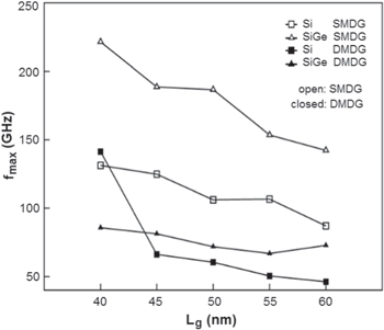
Figure 8. The maximum oscillation frequency fmax versus gate length Lg.
Download figure:
Standard image High-resolution image3.2. Variation in oxide thickness
Figure 9 shows the variations of ft versus Tox. It can be observed that ft increases with decreasing gate oxide thickness for both Si and Si0.6Ge0.4 TFETs. This can be attributed by the improvement in the gate electrostatic integrity over the channel due to the screening of the electric field at the source side [26]. Si0.6Ge0.4 TFETs exhibits higher ft compared to Si TFETs since the former has more gm.

Figure 9. The unity gain cut-off frequency ft versus gate oxide thickness Tox.
Download figure:
Standard image High-resolution imageFigure 10 shows the variations of fmax versus Tox. It can be inferred from the plot that as Tox decreases, fmax increases due to the smaller gate resistance near the source side and the charge carriers are confined only near the drain region [26].
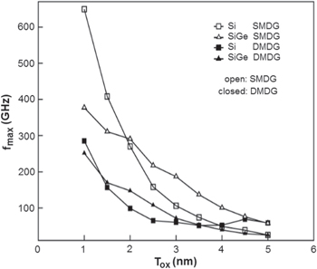
Figure 10. The maximum oscillation frequency fmax versus gate oxide thickness Tox.
Download figure:
Standard image High-resolution image3.3. Variation in channel thickness
Figure 11 shows the variations of ft versus Tch. It can be observed that ft increases with decreasing channel thickness. With the scaling of the channel thickness, screening of gate fringing fields dominates, and reduces gate capacitance which ultimately improves ft [26]. As discussed already, Si0.6Ge0.4 TFETs exhibits higher ft compared to Si TFETs.
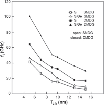
Figure 11. The unity gain cut-off frequency ft versus channel thickness Tch.
Download figure:
Standard image High-resolution imageFigure 12 shows the variations of fmax versus Tch. The increase in fmax can be reasoned out as the reduction in gds for lesser values of channel thickness. This holds the same for both Si and Si0.6Ge0.4 TFETs.
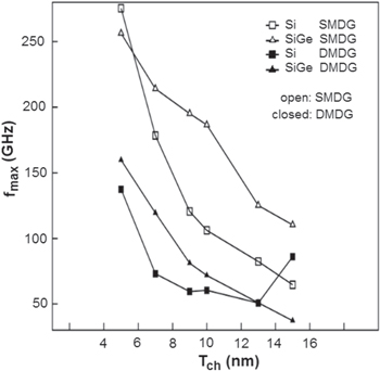
Figure 12. The maximum oscillation frequency fmax versus channel thickness Tch.
Download figure:
Standard image High-resolution image3.4. Variation in underlap
Figure 13 depicts the plot between ft and Lun for Si and Si0.6Ge0.4 SMDG and DMDG TFETs. For all the devices, ft shows a decreased value for the increase in Lun. This may be due to the decreased gm values for larger values of Lun [27, 28].
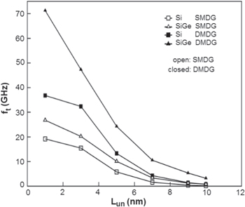
Figure 13. The unity gain cut-off frequency ft versus underlap Lun.
Download figure:
Standard image High-resolution imageFigure 14 shows the variations of fmax versus Lun. The plot depicts the decreased values of fmax for higher values of underlap. The effective channel length is wider for the increased underlap and the inversion layer is formed close to the drain region. This increases gds which ultimately reduces fmax. This effect is seen for both Si and Si0.6Ge0.4 TFETs.
Figure 14. The maximum oscillation frequency fmax versus underlap Lun.
Download figure:
Standard image High-resolution image
4. Conclusion
To enhance ON current for a reduced SS in TFETs, Si1−xGex is optimized and then compared with Si based SMDG and DMDG devices. Four structural parameters—gate length, gate oxide thickness, channel thickness and underlap are considered to study the impact of ft and fmax in Si and Si0.6Ge0.4 SMDG and DMDG TFETs. It can be observed that Si0.6Ge0.4 offers more ft and fmax with respect to the variation in the structural parameters. Higher value of fmax can be attributed to inversion layer formed closely to the drain more than to the source unlike conventional MOSFETs. Hence SiGe TFETs seems to be promising candidate to replace Si TFETs for the future analog/RF applications.
Acknowledgment
This work is supported by Department of Science and Technology, Government of India under SERB scheme (Grant No: SERB/F/2660).