

Abstract
Low dimensional cubic phase ZnS quantum dots (QDs) are formed by mechanical alloying the stoichiometric mixture of Zn and S powders at room temperature. During milling process the primary mixed phase ZnS is formed at about 3.5 h of milling and strain less single phase (cubic) ZnS QDs are formed with ∼4.5 nm in size after 20 h of milling. Detailed microstructure study has been done by both Rietveld analysis of x-ray diffraction pattern and high resolution transmission electron microscope images. Dc resistivity decreases with increasing temperature which can be explained by three-dimensional hopping conduction mechanisms. Observed negative magnetoconductivity has been analyzed by wave function shrinkage model. Alternating current conductivity can be described by the correlated barrier hopping conduction mechanism. Analysis of complex impedance indicates that the grain boundary resistance is found to be dominating over the grain resistance. Relaxation behavior has been explained by the analysis of the electric modulus.
Export citation and abstract BibTeX RIS

Original content from this work may be used under the terms of the Creative Commons Attribution 3.0 licence. Any further distribution of this work must maintain attribution to the author(s) and the title of the work, journal citation and DOI.
1. Introduction
Synthesis of quantum dots (QDs) and their various applications is now seen one of the potential areas of modern day research [1–3] due to their novel electrical and optical properties obtaining from quantum confinement. ZnS has drawn much attention due to its excellent properties such as direct recombination, and resistance to high electric field [4–7]. ZnS QDs are also potentially used in optoelectronic and electroluminiscence devices, solar cells and infrared windows. Due to high luminescence phosphorence properties ZnS QDs are utilized in the field of laser, sensors and displays [8–10]. Though various chemical and physical paths had been adopted to synthesize semiconductor QDs but there are very few report on mechanosynthesis of QDs by mechanical alloying the elemental powders in a single step at room temperature.
In zinc-blende structure (77090-ICSD, Sp. Gr. F-43m.a: 5.434 Å) the cubic ZnS is stable in nanocrystalline form and it converts to hexagonal wurtzite (67453-ICSD, Sp. Gr. P63mc, a: 3.8227 Å; c: 6.260 Å) structure at ∼1020 °C [11]. It is reported in the earlier cases that whatever the methods of preparation are, ZnS QDs always belong to the cubic structure [12, 13]. From the x-ray diffraction (XRD) pattern of ZnS QDs, it is very much difficult to identify the presence of minor hexagonal phase, though the existence of hexagonal phase in small quantity may affect several properties of QDs to a great extent. It is possible to determine the presence as well as quantitative phase estimation of the trivial hexagonal phase in a precise way by considering all its reflections and adopting Rietveld method [14–16] of profile fitting of x-ray powder diffraction spectra based on crystal structure and microstructure refinement methodology. In addition to that, extensive and in-depth study of the XRD pattern of the ZnS QDs by Rietveld method revealed the existence of different kinds of stacking faults, small particle size, change in lattice parameter, residual strain etc [17–19].
Due to large surface to volume ratio and quantum confinement effects, the nanomaterials exhibit novel electrical, magnetic and optical properties as compared to their bulk counterparts. Recently, nanostructures viz., nanoparticles, nanofibers, nanotubes, QD etc have received remarkable attention among the scientific community owing to their potential applications [20–24]. Despite the remarkable progress in the field of nanostructures, both in terms of fundamental and technological viewpoints, charge transport mechanism in such disordered low dimensional structures has not been fully understood. DC resistivity and magnetoconductivity is the primary tool to understand the charge transport mechanism in a material. Impedance spectroscopy is a non-destructive technique to characterize the electrical and charge carrier relaxation behavior of materials under the application of an alternating electric field. The charge transport and charge carrier relaxation behavior are the two fundamental aspects for designing electronic devices. In the present work, we report an in depth analysis of the dc resistivity, magnetoconductivity, ac conductivity and impedance spectroscopic study of the ZnS QDs in the temperature range 77 K ≤ T ≤ 300 K.
2. Experimental procedure
Mechanical alloying (MA) of pure zinc (purity 99.5%, Loba Chem.) and sulphur powders (purity 99.5%, Merck) were carried out at room temperature under Ar atmosphere using a planetary ball mill (model-P5, M/S Fritsch, GmbH, Germany). The progress of milling was monitored at different intervals of time, and changes are noticed in x-ray powder diffraction pattern of ball-milled samples. The x-ray powder diffraction profiles of the unmilled mixture and ball milled samples were recorded using Ni-filtered CuKα radiation from a highly stabilized and automated Philips x-ray generator (PW 1830). All the samples were dispersed in ethanol, sonicated and subsequently, a drop of it was put on a copper grid for microstructures using high resolution transmission electron microscope (HRTEM) operated at 200 kV.
The electrical conductivity of the samples was measured by a standard four probe method after good contact was ensured with highly conducting graphite adhesive (Electrodag 5513, Acheson, Williston, VT) and fine copper wires as the connecting wires. The dc conductivity was measured with an 81/2—digit Agilent 3458A multimeter. The temperature dependence of the conductivity was studied with a liquid nitrogen cryostat. For the control and measurement of the temperature, an ITC 502S Oxford temperature controller was used. To measure the dc response, pellets of 1 cm in diameter of the samples was made by pressing the powder under a hydraulic pressure of 500 MPa. The magnetoconductivity was measured in the same manner by the variation of the transverse magnetic field (B < 1 T) with an electromagnet.
To obtain the optimized structural parameters and microstructure parameters such as particle size, rms lattice strain and stacking faults, we have adopted the Rietveld's software MAUD 2.14 [17] for powder structure refinement analysis of XRD pattern. The simulation was done using cubic ZnS and hexagonal ZnS phases in a single pattern as the patterns are composed of reflections from these phases. Considering the combined intensity of the peaks as a function of structural and microstructural parameters, the Marquardt least-squares procedures were adopted for optimization and the minimization of the difference between the observed and simulated powder diffraction patterns was monitored using the value of goodness of fit (GoF). Refinements of all parameters like particle size, lattice strain values, lattice parameters (including zero-shift error) and stacking fault were continued till convergence is reached with the value of the quality factor, GoF very close to 1 (varies between 1.1 and 1.3), which confirms the goodness of refinement. The more detail analysis of microstructure has been reported in the previous work [25].
3. Results and discussion
All x-ray powder diffraction (XRD) patterns of Zn and S stoichiometric powder mixture prepared at different milling time are shown in figure 1. It clearly shows that the unmilled (0 h) mixture is composed of Zn (JCPDF # 04-0831; hexagonal, Sp. Gr. P63/mmc, a: 2.665 Å, c: 4.947 Å) and sulphur (412326-ICSD, Sp. Gr. Fddd, orthorhombic, a: 10.393 Å; b: 12.762 Å; c: 24.436 Å) phases. In the course of milling time up to 3.5 h, all ZnS reflections emerge clearly in the XRD pattern. The ZnS XRD patterns are identified as the overlapping of both from zinc-blende (cubic) as major phase and wurtzite (hexagonal) as minor phase. Since, there is no significant change except the increase in peak-broadening in all XRD patterns with increasing milling time up to 20 h, it seems that the cubic ZnS is a stable phase and remains invariant up to 20 h of milling. In the present study, the simulated XRD patterns for Rietveld analysis are generated with the following phases: ZnS (cubic), and ZnS (hexagonal). Experimental XRD patterns (figure 2) of ball-milled samples are fitted very well by refining the structural and microstructure parameters of respective simulated patterns. The GoFs in all cases lie in between 1.1 and 1.3 which signify that the fitting qualities are good enough for all experimental patterns. The residual of fittings (IO–IC) between observed (IO) and calculated (IC) intensities of each fitting is plotted under respective XRD patterns. Peak positions of all reflections of ZnS phases are marked (|) and shown at the bottom of the plot. It is clear from the figures 1 and 2 that the degree of overlapping between two phases of ZnS is very high. As the contribution of hexagonal phase is quite small it is therefore very difficult to notice its presence in the XRD patterns. However, the Rietveld analysis of XRD data clearly reveals the simultaneous presence of both cubic and hexagonal ZnS phases and estimates the phase content and other structural/microstructure parameters of this phase which was not possible by any simple technique of XRD data analysis or even by HRTEM alone. The Rietveld analysis of ball-milled samples up to 10 h detects the presence of hexagonal phase and confirms the presence of single cubic ZnS phase after 20 h of milling.

Figure 1. X-ray powder diffraction patterns of unmilled and ball-milled stoichiometric mixture of elemental Zn and sulphur powders (1:1 molar ratio) for different durations under argon medium. ZnS (C) denotes the cubic ZnS phase and ZnS (H) denotes the hexagonal ZnS phase.
Download figure:
Standard image High-resolution image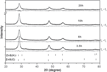
Figure 2. Observed (·) and calculated (−) x-ray powder diffraction patterns of unmilled and ball-milled samples of Zn and sulphur (1:1 molar ratio) powders milled for different durations revealed from the Rietveld powder structure refinement analysis.
Download figure:
Standard image High-resolution imageThe occurrence of different kinds of stacking faults is clearly evidenced in the HRTEM images of 20 h milled sample. The atomic layer shown in the figure 3 is identified as (111) plane of cubic ZnS phase with inter planer spacing d = 3.05 Å. This HRTEM image authenticates the existence of different kinds of staking faults in the ball-milled samples. However, HRTEM image fails to give their concentrations because this image is extremely localized. The concentrations of all three types of stacking faults, intrinsic (α'), extrinsic (α'') and twin (β) among 103 atomic layers have been worked out employing the peak-shift analysis as proposed by Warren and Averbach [18] and adopting the Rietveld software MAUD 2.14 [17] and are given in table 1. The variation in relative phase abundances of ball-milled samples are taken from the Rietveld analysis of XRD data of respective samples and are reported in table 1. It is interesting to note that after the instant formation of both the phases at 3.5 h of milling and after 20 h of milling only single cubic phase is formed. The rapid reduction in particle sizes of all phases in ball-milled sample with increasing milled time is reported in table 1. Initially, after 3.5 h of milling particle sizes of cubic and hexagonal ZnS phases are almost equal and decrease with same manner and size of cubic ZnS phase reduces to ∼4.5 nm after 20 h of milling. It is evident from table 1 that the ball milled sample contains lattice strains. The rms lattice strain produced in both the ZnS phases during the milling has been obtained from the Rietveld analysis. The stable cubic phase is initiated with a less amount of lattice strain and the strain in cubic lattice reduces rapidly almost to zero within 20 h of milling.

Figure 3. HRTEM lattice images of cubic ZnS phase in 20 h ball milled sample showing the presence of different kinds of stacking faults generated in the stacking sequence of (111) plane of cubic particles.
Download figure:
Standard image High-resolution imageTable 1. Variation of different microstructure parameters with increasing milling time obtained from Rietveld analysis for both ZnS cubic [ZnS(C)] and Zns hexagonal [ZnS(H)] phases. Stacking faults are associated among thousand atomic layers.
| Milling time (hour) | Phases | Mol fraction % | Intrinsic stacking fault | Extrinsic stacking fault | Twin fault | Particle size (nm) | rms strain × 103 |
|---|---|---|---|---|---|---|---|
| 3.5 | ZnS(C) | 0.875 | 62.27 | 0.0809 | 10.47 | 41.15 | 10.87 |
| ZnS(H) | 0.125 | — | — | — | 48.675 | 24.6 | |
| 6 | ZnS(C) | 0.88 | 62.52 | 0.4265 | 19.36 | 17.104 | 8.724 |
| ZnS(H) | 0.12 | — | — | — | 10.152 | 11.18 | |
| 10 | ZnS(C) | 0.905 | 38.62 | 0.9297 | 19.55 | 11.938 | 8.15 |
| ZnS(H) | 0.095 | — | — | — | 8.11 | 7.04 | |
| 20 | ZnS(C) | 1 | 11.56 | 1.0194 | 28.31 | 4.557 | 1.98 |
| ZnS(H) | 0 | — | — | — | — | — |
The dc resistivity variation with temperature has been studied in the temperature range 77–300 K for different samples. Resistivity of the samples decreases with increasing temperature; such behavior indicates the prevalence of hopping type charge transport and resistivity variation with temperature can be expressed as [26]

where ρ0 is the resistivity at infinite temperature, γ is an exponent and its value depends on the sample dimension. Its value is 1/2 for one-dimension, 1/3 for two-dimensions and 1/4 for three-dimensions. TMott is the Mott characteristic temperature, which depends on the localization length (Lloc) and density of states (N(EF)) at Fermi surface and can be given by the relation

where kB is the Boltzmann constant. We have used the three-dimentional pellet of the samples for electrical measurement, γ = 1/4 has been useful for analysis the experimental data. In figure 4, the logarithmic resistivity variation with T−1/4 has been shown. A straight line variation established that the three-dimensional hopping conduction is the dominated charge transport of the investigated samples and the value of TMott has been calculated from the slope of the straight lines in figure 4 and listed in table 2. The value of TMott of the zones samples increases with increasing milling time from 3.5 to 20 h.

Figure 4. Variation of the dc conductivity (σdc) with temperature of different samples.
Download figure:
Standard image High-resolution imageTable 2. Values of relevant physical parameters for different milled samples. ρ300 K is the resistivity at 300 K, TMott is Mott characteristic temperature, Lloc is the localization length, Rhop is the hopping range, WH is the effective barrier height and τ0 is the characteristic relaxation time.
| Milling time (hours) | |||||
|---|---|---|---|---|---|
| Parameters | 0 | 3.5 | 6 | 10 | 20 |
| ρ300K (Ω m) | 5.40 × 10⁷ | 8.08 × 10⁷ | 9.33 × 10⁷ | 2.38 × 10⁷ | 1.26 × 10⁷ |
| TMott (K) | 11.60 × 10⁷ | 1.63 × 10⁷ | 3.88 × 10⁷ | 4.57 × 10⁷ | 8.50 × 10⁷ |
| Lloc (nm) | 4.14 | 7.93 | 6.94 | 7.15 | 6.91 |
| Rhop (nm) | 0.06 | 0.19 | 0.14 | 0.14 | 0.11 |
| WH (eV) | 0.54 | 0.65 | 0.77 | 0.89 | 1.04 |
| τ0 (s) | 5.63 × 10⁻⁸ | 4.52 × 10⁻⁸ | 2.10 × 10⁻⁸ | 7.53 × 10⁻⁹ | 6.56 × 10⁻⁹ |
Magnetotransport property of the zones QD samples have been studied within the temperature range 77 K ≤ T ≤ 300 K in presence of transverse magnetic field B ≤ 1 T. We have measured magnetoconductivity which is decreasing with increasing magnetic field i.e. negative magnetoconductivity has been observed for all samples. At magnetic field B = 0.8 T and temperature T = 300 K the maximum percentage changes of conductivity  varies from −1.72% to −5.76%. Figure 5 shows the variation of room temperature magneto conductivity with magnetic field for different samples. Generally, the dc magnetoconductivity of the investigated samples can be analyzed by two simultaneously acting hopping conduction processes like (i) the wave function shrinkage model [27, 28] and (ii) the forward interference model [29–31]. According to wave function shrinkage model, in presence of magnetic field the wave functions of conduction electrons are contracted, which reduces the average hopping length. Hence the conductivity decreases with increasing magnetic field and the magneto conductivity ratio can be presented by the relation [27]

where t1 = 5/2016 and Lloc is the localization length. On the other hand, in case of forward interference model, the forward interference among random paths between two sites has been observed in the hopping conduction processes and resulting the positive magnetoconductivity. Hence the magnetoconductivity ratio can be expressed as

where Csat is a temperature independent parameter and  . Therefore, due to the competition between the wave function shrinkage effects and the quantum interference effects, the sign and magnitude of magnetoconductivity of the investigated samples will be changed. In our observation the negative magnetoconductivity of the investigated samples suggested that the wave function shrinkage effect is predominant over forward interference effect. Therefore, the experimental data have been analyzed by using the wave function shrinkage model. In figure 5 a linear variation of ln[σ(B, T)/σ(0, T)] with B2 for different samples at room temperature are shown. Different points in the figure represent the measured data and the solid straight lines represent the theoretical best fits according to the wave function shrinkage model. From this fitting we may presume that the experimental data are reasonably well fitted with the above theoretical prediction. From the slopes of each straight line we have calculated the localization length for different samples which lies in the range 4.14–7.93 nm. The small value of localization length has been observed due to presence of strong disorder in the QD samples having high resistivity at room temperature. The variation of negative magnetoconductivity of 20 h milled sample with magnetic field at different but constant temperatures is shown in figure 6. The observed negative magnetoconductivity has been analyzed by using the theory of wave function shrinkage effect. In figure 6 the points are the experimental data and the curve is the theoretical best fit with wave function shrinkage model. The localization length has been calculated from the slopes of the graphs at different temperatures and the value increases from 3.84 to 6.91 nm with increasing temperature 77–300 K. Due to the small localization length of QD, the average hopping length
  is small and its value at 300 K varies from 0.06 to 0.19 nm for different samples but its value increases from 0.04 to 0.11 nm with increasing temperature from 77 to 300 K for 20 h milled samples. Such low values of hopping length suggest that the wave function shrinkage effect is prominent in QD samples and observed magnetoconductance is negative.
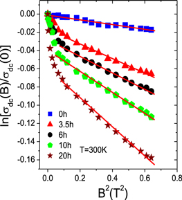
Figure 5. Variation of the dc magnetoconductivity with perpendicular magnetic field of different samples at 300 K.
Download figure:
Standard image High-resolution image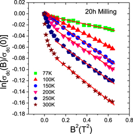
Figure 6. Variation of the dc magnetoconductivity with perpendicular magnetic field of the S5 sample at different temperatures.
Download figure:
Standard image High-resolution imageThe total frequency dependent conductivity has been measured at constant temperatures of all the samples. At a particular temperature, the total frequency dependent conductivity shows two distinct behaviors like a weak frequency dependent behavior due to dominant dc conductivity at lower frequency. On the other hand at higher frequency conductivity strongly depends on frequency and follows the power law of frequency. In this case the total frequency dependent conductivity can be expressed as the sum of the ac (σac) as well as dc (σdc) conductivity [26, 32, 33] and can be written as

where α is the temperature dependent constant and s is the frequency exponent. In figure 7 we have plotted ln[σac(f)] with ln(f) which shows the straight line variation. For different temperatures the values of 's' have been calculated from the slope of each straight line. The variation of 's' with temperature for different samples has been shown in figure 8. It is observed that the values of 's' decreases with increasing temperature. In case of amorphous semiconductors, the temperature dependence of 's' has been reported by different theoretical models [32–34] where the functional form of 's' with temperature is different for different conduction models. Considering all the models and comparing with the observed temperature variation of 's', correlated barrier hoping (CBH) model is suitable conduction processes. According to this model, the charge carriers hop over the potential barrier between two charged defect states and the variation of 's' with temperature can be expressed as [34]

where 
 and
and  are the effective barrier height, angular frequency and characteristic relaxation time respectively. The variation of 's' with temperature for different sample has been shown in figure 8, where the different points are the experimental data and the solid lines are the theoretical best fit with the equation (6) taking
  and
and  as fitting parameters. Hence the experimental data are well fitted with the theoretical prediction obtained from CBH model. The best fitted values of the parameters
  and
and  at 10 KHz are lying in the range 0.54–1.05 eV and 5.63 × 10⁻⁸–0.66 × 10⁻⁸ s, respectively, for different samples. It is observed from the analysis that the value of effective barrier height increases with increasing milling time, whereas the characteristic relaxation time decreases with increasing milling time. Considering all the above facts, we may conclude that the ac conduction mechanism of all investigated samples is corroborated by the CBH model.
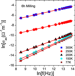
Figure 7. Variation of ac conductivity with frequency at different temperatures.
Download figure:
Standard image High-resolution image
Figure 8. Thermal variation of the frequency exponents for different samples.
Download figure:
Standard image High-resolution imageFor a particular frequency, the temperature dependence of real part of dielectric permittivity of  for the 20 h milled sample has been shown in figure 9, where no sharp peak has been observed within the maximum possible investigation temperature range. It is observed from the figure that the real part of dielectric permittivity increases monotonically with temperature and follows a power law behavior
  Different points are the experimental data at different frequencies and the solid lines are the theoretical best fitted values in accordance with the power law. The fitting yields the values of temperature exponent n which depends strongly on the frequency (its value decreases with increasing frequency). According to the figure the variation of the
  with temperature at lower frequency is dominating over the variation at higher frequency. In disordered semiconductor, interfacial polarization has been observed due to structural inhomogenities. Hence the hopping electron may be trapped by the inhomogenities at low frequencies. However by increasing temperature, the resistance of the composites decreases and electron hopping is promoted by the low resistance. As a result an enhanced polarizibility or larger
  has been observed with temperature for a particular frequency.
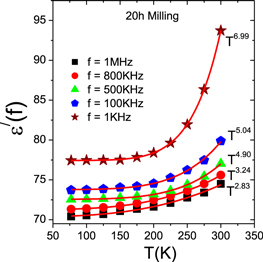
Figure 9. The temperature variation of real part of complex dielectric constant at different frequencies.
Download figure:
Standard image High-resolution imageIn order to find out the grain and grain boundary contribution of such inhomogeneous system, the complex impedance can be analyzed by an equivalent circuit containing grain and interfacial grain boundary resistances and capacitances and can be expressed as [35, 36]


where C0 is free space capacitance, Rg, Rgb, Cg and Cgb are grain and interfacial grain boundary resistance and capacitance, respectively. By using the real  and imaginary
  part of dielectric constant, the real part of the complex impedance can be calculated by using the relation

At room temperature, the variation of real part of complex impedance has been shown in figure 10 for different samples. The grain and grain boundary resistance and capacitance have been calculated by least square fitting of experimental data with equation (10) taking Rg, Rgb, Cg and Cgb as fitting parameters. In figure different points are the experimental data whereas the best fitting is represented by solid lines. The best fitted values of the parameters are lying in the range 2.23–280.93 KΩ for Rg, 0.14–0.48 nF for Cg, 7.28 KΩ–5.68 MΩ for Rgb and 0.22–5.67 nF for Cgb for different samples. It is observed that the values of Cgb and Cg have the same order of magnitude, however the values of Rgb for different samples are greater than the values of Rg. This implies that the grain boundary contribution dominates over the grain contribution. In figure 11, variation of real part of complex impedance with frequency in presence and in absence of magnetic field at different temperature has been shown. It is observed from the figure that below the 10 kHz frequency the impedance of the sample is greater than the values obtained without magnetic field. This is because at lower frequency long range conductions are favorable, so the applied magnetic field may influence more on the carrier motion which results more positive impedance by application of magnetic field at lower frequencies. From analysis of the real part of complex impedance data with equation (8) we have calculated the grain and grain boundary contribution in presence of constant magnetic field B = 0.8 T. It is observed from the calculation that the total contribution due to grain and grain boundary resistances (R = Rg + Rgb) increases from 5.83 to 25.80 MΩ at 300 K and 24.96 to 53.77 MΩ at 77 K in absence and in presence of magnetic field 0.8 T, respectively. So we may presume that the influence of the magnetic field on the impedance is due to the change of grain and grain boundary resistances by the applied magnetic field.

Figure 10. The real part of the complex impedance versus frequency of different samples at 300 K.
Download figure:
Standard image High-resolution image
Figure 11. The real part of the complex impedance versus frequency in presence and in absence of magnetic field: (a) at 300 K and (b) at 77 K.
Download figure:
Standard image High-resolution imageAnalysis of the dielectric properties of the samples by the complex electric modulus formalism has been done to avoid the electrode effect [37]. The complex electric modulus (M*(f)) can be described by the relation
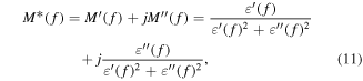
where  and
and  represent the real and imaginary components of the complex electric modulus respectively. The variation of real and imaginary components of complex electric modulus with frequency is shown in figure 12 for different samples. From the figure it is noticed that the value of
  increases with increasing frequency and undergoes a step like change. It is also observed in figure 12 that the step like change in
  versus f curve is accompanied by a relaxation peaks in
  versus f curve. The relaxation peaks are not observed for temperature T < 300 K. The peak frequency has an importance because the charge carriers freely move below the peak frequency and are confined above this frequency [38, 39]. It is observed in figure 12 that for a particular temperature, the peak position is shifted to higher frequency due to increase of milling time. With increasing milling time the hexagonal phase ZnS is converted to cubic phase and the sample is fully cubic phase after 20 h of milling. Hence the measured conductivity increases i.e. mobility of the free charges increases and relaxation time decreases. As a result the peak position moves toward the higher frequency with increasing milling time.

Figure 12. Variation of real and imaginary part of electric modulus with frequency at 300 K for different samples.
Download figure:
Standard image High-resolution image
4. Conclusion
ZnS QDs with cubic phase can be prepared by top-down physical method of MA at room temperature. Initially along with major cubic ZnS phase the amorphous like minor hexagonal ZnS phase is formed and in the course of milling up to 20 h, the single phase cubic ZnS is formed with ∼4.5 nm in size and almost free from lattice strain. The existence of different kinds of stacking faults in ball-milled samples are estimated by the Rietveld method which is also approved by the HRTEM images and thereby an well rationalization between direct and indirect observation techniques is noticed. Resistivity of the samples decreases with increasing temperature, which indicates the prevalence of three-dimensional hopping type charge transport. The negative magnetoconductivity of the investigated samples suggested that the wave function shrinkage effect is predominant over forward interference effect. The localization length increases from 3.62 to 6.52 nm with increasing temperature. At higher frequency conductivity strongly depends on frequency and follows the power law of frequency. Hence the ac conduction mechanism of all investigated samples is corroborated by the CBH model. Relaxation properties of the samples have been described by the analysis of the electric modulus. Analysis of the complex impedance by an equivalent circuit containing grain and interfacial grain boundary resistances and capacitances implies that the grain boundary contribution dominates over the grain contribution.
Acknowledgments
The authors gratefully acknowledge the principal assistance received from the MHRD, Government of India during this work.