

Abstract
In the present work, nanostructured ZnO doped with  (2, 4, 6, 8 and 10
  ) is prepared by conventional solid state reaction method. X-ray diffraction peak intensities are sharp and narrow, confirming that the sample is of high quality with good crystallinity. The intensity and full width at half-maximum of x-ray diffraction peaks of (100) and (101) decreases with the increase of
  dopant in ZnO. X-ray peak profile analysis was used to evaluate the crystallite size and lattice strain by the Williamson-Hall (W-H) method. Using the models namely uniform deformation model (UDM), uniform stress deformation model (USDM) and uniform deformation energy density model (UDEDM) of W-H method, the physical parameters such as strain, stress, and energy density values were calculated. The surface morphology and elemental composition of the samples were characterized by scanning electron microscope and energy dispersive spectroscopy.
Export citation and abstract BibTeX RIS

Original content from this work may be used under the terms of the Creative Commons Attribution 3.0 licence. Any further distribution of this work must maintain attribution to the author(s) and the title of the work, journal citation and DOI.
1. Introduction
Zinc oxide (ZnO) has been considered as one of the most promising materials for optoelectronic applications due to its wide energy band gap of 3.37 eV, large exciton binding energy of 60 meV, high optical gain, and high radiation and temperature stability [1]. In order to extend the application possibility of ZnO-based devices, several doping elements have been studied and reported, such as Ga, N, In, and Sn. However, it is difficult to achieve  type doping in ZnO. Recently, there were reports indicating that doping with group V elements, such as phosphorous (P), arsenic (As), and antimony (Sb) was achieved, and the
  type materials exhibited superior electrical properties [2]. Among the group V elements, antimony has similar ionic radius to that of Zn ion [3]. Some reports suggested that doping with antimony might produce more stable
  type conductivity and higher carrier concentration [4, 5]. Antimony oxide
  had a wide band gap of 3.4 eV, which is widely used in various applications as catalyst, flame retardant, optoelectronic and photoelectric devices [6]. The photocatalytic activity of pure
  is low due to high band gap
  [7]. The coupling of
  with other metal oxides can effectively improve the photocatalytic activity. Recently,
  doped ZnO microflowers have been deposited onto tiny
  chip to fabricate a smart chemical sensor for toxic ethanol [8]. The present work is devoted to understand the microstructural properties of
  doped ZnO. However, the x-ray peak profile analysis of
  with ZnO has not yet been reported. X-ray peak profile analysis (XPPA) is used to estimate the micro-structural quantities and correlate them to the material properties. It is a simple and powerful tool to estimate the crystallite size and lattice strain [9]. The lattice strain and crystallite size affect the Bragg peak in different ways and both these effects increase the Bragg peak width, peak intensity and shift the
  peak position accordingly. The pseudo-Voigt function, Rietveld refinement, and Warren-Averbach analysis are used to estimate the lattice strain and crystallite size [10–12]. However, the Williamson-Hall (W-H) analysis is a simplified integral breadth method employed for estimating crystallite size and lattice strain, considering the peak width as a function of
  [13, 14]. In the present work, XPPA is carried out to estimate the crystallite size, strain, stress and strain energy density of
  doped ZnO nanoparticles based on modified W-H plots using uniform deformation model (UDM), uniform stress deformation model (USDM), and uniform deformation energy density model (UDEDM). A detailed study using these models on ZnO doped with different concentrations of
  samples is not reported yet. This study reveals the importance of W-H models in the determination of crystallite size and strain of
  -doped ZnO nanocomposite semiconductors.
2. Experimental details
Nanostructured ZnO doped with 2%, 4%, 6%, 8% and 10% of  were synthesized by conventional solid-state reaction method. The appropriate ratio of the constituent oxides, i.e. ZnO and
  (99.99% Aldrich Chemicals, USA) were milled in a planetary ball miller (Retsch PM 200) with tungsten carbide milling media (10 mm diameter balls) at a ball-to-powder weight ratio of 10:1 and at a speed of 350 rpm for 12 h. These mixed powders was calcined at
  for 10 h and finally sintered in a programmable SiC furnace at
  for 3 h with a heating and cooling rate of
  . The x-ray diffraction (XRD) patterns of the prepared samples were recorded at room temperature using Philips: PW 1830 with
  radiation
  in a wide range of Bragg angles
  with scanning rate of
  . The pseudo-Voigt function which is a linear combination of a Lorentzian and Gaussian function was used in order to obtain the information about the shapes and integrated intensities of Bragg reflections for the investigated samples. The diffraction lines were modelled by pseudo-Voigt functions and the background by a fifth-order polynomial. The following parameters were refined: the overall scale factor; the background (six parameters of the 5th order polynomial);
  Zero; the unit cell parameters; the specimen displacement; the half-width parameters; the peak shape; the reflection-profile asymmetry; the Lorentzian isotropic strain; the isotropic thermal parameters. Also the preferred orientation parameters were refined in order to obtain a good fit of the calculated diffraction pattern. The surface morphology of the samples has been carried out by scanning electron microscope (SEM) (Model: Carl Zeiss, EVO MA15) instrument operated at 15 kV with a resolution of 3.5 nm. The elemental composition of ZnO doped with
  was determined from energy dispersive x-ray spectroscopy (EDS) which is attached to SEM.
3. Results and discussion
3.1. Structural properties
XRD patterns of ZnO doped with different concentrations of  are shown in figure 1. The diffraction peaks at
  and
and  are marked by their miller indices (100), (002), (101), (102), (110) and (103), corresponding to ZnO (space group p63mc, JCPDS no. 36-1451) indicating that the phase of the sample was wurtzite structure. XRD peaks corresponding to the
  (JCPDS no. 74-1858) phase were observed, which indicates that the structure shift from mono phase to heterophase. The intensity of these peaks increased with the increase of doping concentration of
  in ZnO. The second phase
  plays an important role in the microstructure development [15]. The intensity of the diffraction peaks (100) and (101) decreased and their full width at half-maximum (FWHM) increased with the increase of
  doping concentration in ZnO. Such changes in crystallinity might be the result of changes in the atomic environment due to impurity doping on ZnO samples. No change in the crystalline structure was noticed, which suggests that the most Sb atoms were incorporated in ZnO wurtzite lattice. Sb dopant in ZnO lattice was expected to substitute Zn atom and connect two vacancies of Zn to form a
  complex [16]. According to Xiu et al [17] the complex
  could be the explanation of strong
  type conductivity in Sb doped ZnO films. This result is attributed to a small lattice mismatch between radii of
  (0.074 nm) and
  (0.076 nm), and it indicates that Sb ions systematically substituted Zn ions without deteriorating its crystal structure.
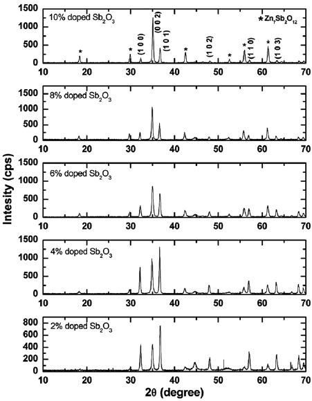
Figure 1. XRD patterns of ZnO doped with different concentrations of  .
.
Download figure:
Standard image High-resolution imageThe average crystallite size  was calculated using Scherrer's formula [18]
where  is crystallite size,
  is shape factor and
  is the wavelength of
  radiation. The crystallite size estimated from Scherrer formula is found to be decreased from 56 to 32 nm with the increase of
  content in ZnO. The decrease of crystallite size correlates with a large developed surface of grain boundaries, thus leading to a larger scattering effect. Another reason for the decreased crystallite size values may be due to the drag force exerted by the dopant ions on boundary motion and grain growth. The increase of
  doping progressively reduces the concentration of zinc in the system. Thus the diffusivity is decreased in ZnO, which results in a suppressed grain growth of
  doped ZnO samples. At the same time, the substituted Sb ions provide a retarding force on the grain boundaries. If the retarding force generated is more than the driving force for grain growth due to Zn, the movement of the grain boundary is impeded [19, 20]. This in turn gradually decreases crystallize size with increasing
  concentration. There exist reports of similar trend in some Mn doped ZnO systems [21, 22].
The lattice parameters  and
and  of ZnO doped with different concentrations of
  were calculated from the positions of the (100) and (002) peaks, respectively using the formulas as reported in our previous work [23]. The lattice constants calculated from XRD data for
  doped ZnO composite samples are close to the lattice constants given in the standard data (JCPDS no. 79-2205, 80-0075). The change in the lattice parameters of ZnO host material depends on the ionic radii of the impurity that substitute the Zn ions at the lattice site [24]. In case of Sb doping the ionic radii of the
  (0.076 nm) is larger than
  (0.074 nm). If
  ion substitutes
  ion in ZnO host lattice, then the variation in the lattice constants is expected due to ionic radii difference which has also been reported in the previous literature [25]. The increase in lattice constant values with increasing
  concentration in ZnO is due to interstitial position of Sb ions in ZnO lattice.
The volume of the ZnO hexagonal cell was calculated using the formula

The Zn–O bond length was calculated from the formula [26, 27]
In wurtzite structure, the parameter  is given by
The degree of crystallinity  was calculated using the following equation
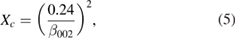
where  is the full width at half maximum (in degrees) of (002) Miller's plane. The unit cell volume is calculated for all samples using lattice parameters. The values of the unit cell volume are increasing with increasing
  concentration in ZnO which led to increase the bond length. The parameter
  represents the relative position of two hexagonal close-packed sublattices i.e. the position of the anion sublattice with respect to the cation sublattice. The enhancement of parameter
  represents the softer Zn-O bond along the
  axis direction.
The specific surface area of the crystallites of the samples was determined from XRD data. The specific surface area is a material property of solids which measures the total surface area of the crystallites present in per unit of mass. It is particularly significant for adsorption, heterogeneous catalysis, and reactions on surfaces. The specific surface area can be calculated by Sauter formula [28]

where  is the specific surface area,
  is the size of the particle and
  is the density of bulk ZnO which equals to
  . The specific surface area of the samples increases with the increase of
  concentration in ZnO. The increase in specific surface area is due to presence of pores (as we noticed in SEM images) which leads to decrease in particle size. The structural parameters of different concentrations of
  doped ZnO estimated from x-ray diffraction data are given in table 1.
Table 1. Microstructural parameters of ZnO doped with different concentrations of  .
.
% of  in ZnO in ZnO |
 (nm) (nm) |
  |
  |
 |
  |
  |
 |
  |
|---|---|---|---|---|---|---|---|---|
| 2 | 62.3 | 3.261 | 5.226 | 1.602 | 48.12 | 1.98 | 0.6663 | 17.1 |
| 4 | 57.2 | 3.361 | 5.272 | 1.568 | 51.57 | 2.03 | 0.6486 | 18.7 |
| 6 | 49.4 | 3.414 | 5.312 | 1.555 | 53.61 | 2.06 | 0.5521 | 21.6 |
| 8 | 46.2 | 3.452 | 5.386 | 1.560 | 55.58 | 2.08 | 0.4162 | 23.1 |
| 10 | 44.1 | 3.486 | 5.412 | 1.552 | 56.95 | 2.10 | 0.3376 | 24.2 |
3.2. Williamson-Hall (W-H) methods
The broadening of XRD pattern is attributed to the crystallite size-induced or strain induced broadening. The significance of peak broadening of the sample evidence the large strain associated with the powder and grain refinement. The instrumental broadening  of the diffraction peak was corrected using the equation

The strain induced in powders due to crystal imperfection and distortion was calculated using the formula [29]
The strain and particle size contributions to x-ray peak broadening are independent to each other and both have a Cauchy-like profile, the observed line breadth is simply the sum of equations (1) and (8)
By rearranging the above equation
The above equations (9) and (10) are Williamson-Hall equations.
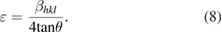
To make Williamson-Hall analysis, a plot is drawn with  along the
  axis and
  along the
  axis for all orientation peaks of
  doped ZnO nanoparticles as shown in figure 2. The crystalline size
  was estimated from the
  intercept and the slope of the linear fit to the data gives the value of strain
  . Equation (10) represents the uniform deformation model, where the strain
  is considered to be uniform in all crystallographic directions. It is clear that there is an increase in the lattice strain with increasing doping concentrations of
  in ZnO. The uniform deformation model for different concentrations of
  doped ZnO is shown in figures 2(a)–(e).
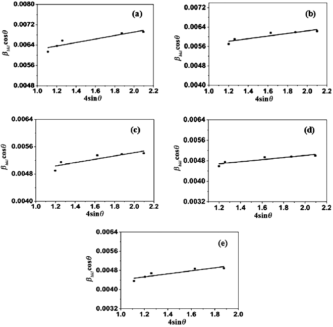
Figure 2. W-H analysis of ZnO doped with (a) 2%  , (b) 4%
  , (c) 6%
  , (d) 8%
  and (e) 10%
  assuming UDM.
Download figure:
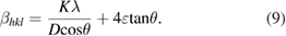
Standard image High-resolution imageIn the uniform stress deformation model (USDM) there is a linear proportionality between stress and strain given by  which is known as the Hook's law within the elastic limit. In this relation,
  is the stress of the crystal and
  is the Young's modulus. Hook's law is a reasonable approximation to estimate the lattice stress. In USDM, the Williamson-Hall equation is modified by substituting the value of strain
  in the second term of equation (5) which yields
 is the Young's modulus in the direction perpendicular to the set of crystal lattice plane
  . The uniform deformation stress is estimated from the slope of the line plotted between
  and
and  , and crystallite size
  from the
  intercept as shown in figure 3.
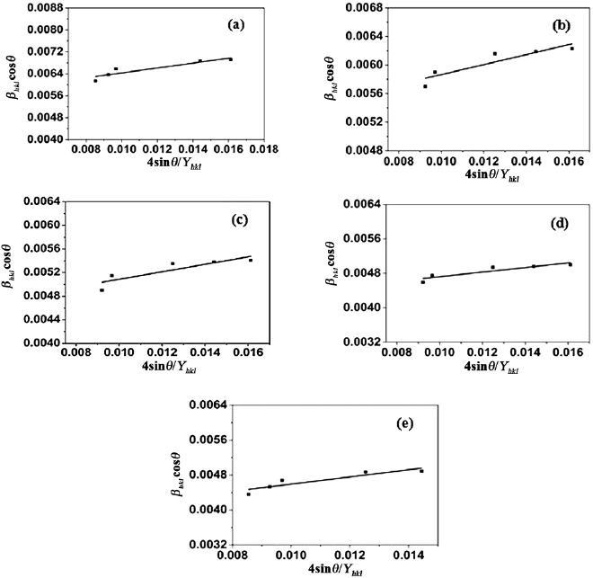
Figure 3. W-H plots of ZnO doped with (a) 2%  (b) 4%
  , (c) 6%
  , (d) 8%
  and (e) 10%
  assuming USDM.
Download figure:
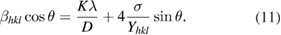
Standard image High-resolution imageThe strain can be measured if  of hexagonal ZnO nanoparticles is known. The Young's modulus
  for hexagonal crystal phase is related to their elastic compliances
  as [30, 31]
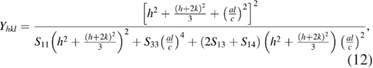
where  ,
,  ,
,  and
and  are the elastic compliances of ZnO and their values are
  ,
,  ,
,  and
and  , respectively [32, 33]. The elastic compliances
  and
and  represent the longitudinal coefficients along the [1000] and [0001] directions, while the
  dominate the transverse modes along the [0001] and [1000] directions. Additionally,
  describes the velocity of modes in low symmetrical directions like [0011]. The Young's modulus,
  value for hexagonal ZnO is
  .
.
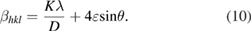
When the strain energy density  is considered, all the constants of proportionality associated with the stress-strain relation are independent. According to Hooke's law, the energy density
  (energy per unit volume) as a function of strain is
  . Thus the equation (11) can be modified to the form
The slope of the line plotted between  and
and  gives the value of uniform deformation energy density. The lattice strain can be evaluated by knowing the
  values of the sample. The value of
  was calculated from the slope and the crystallite size
  is estimated from the
  intercept of linear fit W-H equations modified assuming UDEDM and the corresponding plots are shown in figure 4.

Figure 4. W-H analysis of ZnO doped with (a) 2%  , (b) 4%
  , (c) 6%
  , (d) 8%
  and (e) 10%
  assuming UDEDM.
Download figure:
Standard image High-resolution imageFrom equations (11) and (13), the deformation stress and deformation energy density are related as  . It is to be note that though both equations (11) and (13) are taken into account in the anisotropic nature of the elastic constant, they are essentially different. This is because in equation (7), it is assumed that the deformation stress has the same value in all crystallographic directions allowing
  to be anisotropic, while equation (12) is developed by assuming the deformation energy to be uniform treating the deformation stress
  to be anisotropic.
The scattering of the points away from the linear expression is lesser for figure 2 as compared with figures 3 and 4. The results obtained from W-H models (UDM, USDM and UDEDM) are summarized in table 2. It can be noted that the values of the average crystallite size obtained from the UDM, USDM and UDEDM are in good agreement with the values obtained from Scherrer's formula. It was observed that the strain and stress values increased with decreasing average crystallite size. This study reveals the importance of models in the determination of crystallite size of  doped ZnO nanoparticles. Thus all the three models are found to be suitable for the determination of crystallite size.
Table 2. Estimated microstructural parameters of ZnO doped with  .
.
% of  in ZnO in ZnO |
Williamson-Hall method | ||||||||
|---|---|---|---|---|---|---|---|---|---|
| UDM | USDM | UDEDM | |||||||
 (nm) (nm) |
  |
 (nm) (nm) |
  |
 (MPa) (MPa) |
 (nm) (nm) |
  |
 (MPa) (MPa) |
  |
|
| 2 | 62.3 | 0.330 | 61.8 | 0.349 | 42.4 | 61.8 | 0.405 | 64.1 | 32.4 |
| 4 | 57.2 | 0.410 | 57 | 0.419 | 53.3 | 57.3 | 0.510 | 64.7 | 33 |
| 6 | 49.4 | 0.487 | 49.2 | 0.502 | 63.3 | 49.3 | 0.556 | 70.6 | 39.3 |
| 8 | 46.2 | 0.538 | 45.8 | 0.558 | 70 | 45.8 | 0.585 | 74.2 | 43.4 |
| 10 | 44.1 | 0.680 | 44.4 | 0.703 | 89.3 | 45.3 | 0.680 | 83.8 | 55.4 |
3.3. Surface morphology and elemental analysis
Figures 5(a)–(e) shows the SEM images of different concentrations of  doped ZnO. The surface morphologies of the samples appeared to be smooth and dense with a lot of pores. It is also observed that the surface of the sample is dense up to 6% doped
  in ZnO, as
  content is increased up to 10
  , the surface is bumpy and rough. Figures 6(a)–(e) shows the EDX spectra of different concentrations of
  doped ZnO. The spectra revealed the presence of Zn, Sb and O elements along with their atomic percentage composition. The presence of O
  peak at 0.56 keV, Zn
  peak at 1.01 keV, Zn
  peak 8.68 keV, Sb
  peak at 3.64 keV was observed. To study the distribution of Sb in the nanostructures, we performed elemental mapping for the samples. It is noticed that the distribution of zinc in the sample was homogeneous, oxygen and antimony remained inhomogeneously distributed. With the increase of Sb concentration, the concentration of zinc decreased significantly. We believe the incorporated Sb atoms substitute Zn atoms from their lattice sites in ZnO nanostructures.
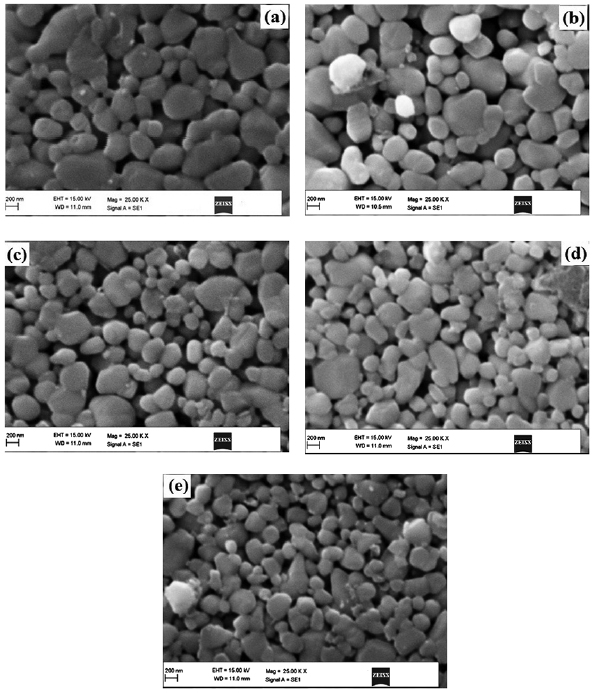
Figure 5. SEM images of ZnO doped with (a) 2%  , (b) 4%
  , (c) 6%
  , (d) 8%
  and (e) 10%
  .
.
Download figure:
Standard image High-resolution image
Figure 6. EDX spectra of ZnO doped with (a) 2%  , (b) 4%
  , (c) 6%
  , (d) 8%
  and (e) 10%
  .
.
Download figure:
Standard image High-resolution image
4. Conclusions
ZnO doped with different concentrations of  samples were prepared by solid state reaction method. Structure analysis indicates that Sb ions substitute for Zn ions without changing the wurtzite structure. The x-ray peak profile analysis is performed for the estimation of crystallite size and lattice strain. The peak broadening was analyzed by the Scherrer's equation and modified forms of W-H models viz. UDM, UDSM, and UDEDM. Hence these models are highly preferable to define the crystal perfection. A modified W-H plot has been used to determine the crystallite size, strain-induced broadening due to lattice deformation and energy density value with a certain approximation. The average crystallite size estimated from Scherrer's formula and W-H analysis shows a small variation because of the difference in averaging the particle size distribution. The strain values obtained from the graphs plotted for various forms of W-H analysis, i.e. UDM, USDM, and UDEDM were found to be accurate and comparable.