
Abstract
Radio-Frequency IDentification (RFID) is a technology that has been emerging for less than a decade as the primary choice to exchange information between objects and their environment. Most of the challenges arise due to the passive nature of the tags placed on objects. The absence of a local power source implies that power management is critical for efficient work of the data exchange link. This paper presents the platform under development at the Laboratory for Nanotechnology to study these challenges. The primary goal of the platform is to implement the complete chain from design and simulation of tags to antenna measurements and field tests of tags through fabrication of real tags on flexible substrates. This structure allows for fundamental and practical studies of new concepts in sensing and wireless networks based on passive tags. A description of the actual achievements is also included.
Export citation and abstract BibTeX RIS

Content from this work may be used under the terms of the Creative Commons Attribution-NonCommercial-ShareAlike 3.0 licence. Any further distribution of this work must maintain attribution to the author(s) and the title of the work, journal citation and DOI.
1. Introduction
Radio-Frequency IDentification (RFID) is a technology that is primarily aimed at object identification. The type of object can range from access control cards, anti-theft stickers or laundry control to the more generally employed logistic tags. This last type of tag allows for tracking goods from pallets to bags in airports. RFID technology spread when Wall-Mart in the USA decided to implement a programme for complete centralized management of the products that it resells [1]. The most important applications of RFID in the public arena are for animal tracking (food safety) [2], supply chain management [3] and contactless access to transportation systems (see [4] with interesting examples from the Seoul bus network, among others). In this paper, we focus on passive RFID, where a tag has to be externally powered by a reader to become active. A lot of applications are in this area because more and more large international companies request that their suppliers use RFID passive tags attached to the goods that they purchase (traceability from the supplier to the end user).
A passive RFID system is composed of two parts: a reader that is linked to the central information system and provides the wireless link with the second part of the system, the passive tag. The latter is affixed to an object or held by a user (access control application). The passive tag is composed of two parts: an antenna to the terminals of which a microchip is connected. The tag is designed so as to be able to extract power from the incoming electromagnetic wave from the reader to power the chip. This allows the chip to handle requests coming from the reader. The exchange of data between the reader and the tag is mainly a set of requests from the reader and replies from the tag through providing the necessary data. Some tags are also writable, as with contactless payment systems, for example, where the amount to be paid should be deduced from the balance stored in the tag.
There exist several electromagnetic bands used for RFID. They are located in ISM (Industrial, Scientific and Medical) bands of the spectrum. The low frequency (LF) band in the range of 125 kHz is specific for low-end applications, such as farm animal tracking. The high frequency (HF) band at 13.56 MHz and the ultra high frequency (UHF) bands in the range of 860–960 MHz are the most used and are developed for real applications. Roughly speaking, the HF band is more dedicated to short range RFID (up to 50 cm) and the UHF band serves the longer range (up to 5 m) identification purposes. Finally, the microwave (MW) band around 2.45 GHz represents interesting potential for the future but is still underdeveloped and few commercial systems are available.
Starting almost two years ago, the goal at the Laboratory for Nanotechnology (LNT) is to develop a platform to cover the important aspects of RFID technology. The idea behind this is to provide in Vietnam a complete research and education platform for the development of new applications of this important technology and training of professionals in its fundamentals. As is evidenced from the application examples given above, RFID is a hidden technology seldom known to the public but it is around in everyday life. This means that professionals are required to at least implement the technology, if not to further its development.
The RFID platform at LNT covers all aspects of RFID technology on the hardware side: design of passive tags, prototype laboratory scale fabrication of tags, reader programming and field test measurements. However, the software part of the technology is very broad and far from the core activity of the laboratory, such that there is only first level activity related to standard programming of RFID readers for technological demonstration purposes. This paper describes the different parts of the platform with a specific emphasis on UHF passive tag development and the actual achievements towards a complete prototyping capability.
2. Platform structure
2.1. Tag design
A passive UHF tag is a resonant system. The antenna and chip electrical circuit is comparable to an inductance–capacitance circuit and it will absorb electromagnetic energy at its resonance. But a tag never exists on its own and is intended to be fixed to something. This implies that its electrical parameters will be influenced by the surrounding materials. Here lies the difficulty for the technology to adapt to multiple practical cases. At present, no tag can claim to be truly universal. Designing UHF tags is thus an integral part of the development of RFID technology.
The progress in simulating electromagnetic systems allows the capability to simulate an RFID system, from the antenna alone [5], a tag with its chip to the complete system (reader and tag, example privately provided by CST). An equivalent electrical model for the chip is enough for a realistic simulation of the tag. In our work, the simulations of our tags are done using Microwave Studio edited by CST. With a complete set of tools, this software allows for a full analysis of computed electromagnetic fields. This makes it easier for the iterative optimization of RFID tags. Indeed, one of the main difficulties in electromagnetic antenna based design is the absence of complete analytical models to predict the behaviour of the system. Therefore, simulation is a mandatory step and can only be done through a trial and error process guided by the analysis of the simplest systems, such as fundamental dipole antenna.
Few basic antenna types exist for UHF RFID tag design, i.e. dipole, meander and slot antennas compatible with the needs of an omnidirectional antenna for most applications [6]. Based on these primary antennas, it is possible to test variations in order to meet a specific target. Such a target may be a broadband small antenna, specific antenna shape (e.g. highly bent type), metal object tagging [5, 7, 8]. A description of the actual challenges facing RFID UHF tag design is, however, beyond the scope of this paper. Figure 1 shows an example of a meander antenna tag with dimensions of 20×40 mm. This is a good example of a narrow band tag dedicated to the first UHF band in Vietnam nearly equivalent to the European standard (ETSI).
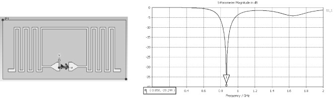
Figure 1 Example of a meander tag designed at LNT and its frequency response.
When it comes to optimizing a tag for practical application purposes, it becomes obvious that the simulation step should take into account the process influence in the real tag. For example, there is the need to connect the chip to the antenna. As will be described in section 2.2, this is the most critical reliability point. Whatever the actual process, there will be an added resistance and capacitance to the overall electrical circuit (to be measured experimentally). Being able to integrate the influence of this connection into the simulation process is key to a real design. Other parameters, such as antenna line resistivity or surface roughness, can also be taken into account to reach a design as close as possible to a final fabricated tag.
2.2. Tag fabrication
Most of laboratories working in the RFID field obtain their tags on FR4 or equivalent PCB materials. Although interesting for fundamental studies, this does not allow for proof-of-concept design of UHF tags. The capability of LNT as a technology laboratory is here leveraged to fabricate tags on flexible substrates. These tags can be used in real-world applications but their fabrication process stays at the laboratory level. At present, real UHF tags are produced in very large quantities by roll-to-roll equipment in order to achieve very low costs. These production tools are out of reach for a research laboratory. Therefore a trade-off is found to fabricate tags on flexible substrates with standard microfabrication tools at the laboratory level.
The category of substrates of interest is the flexible polymer films. These offer availability at low cost and conformable advantages for demonstration purposes. Unfortunately, standard plastic films, such as PET or polyesters, show low processing temperature capability and here lie the challenges for RFID tags: a low-cost tag on a substrate that is not easy to process. At this stage, we focus on commercially available PET films. We chose 80 μm thick films purchased without any specific finish. These films are carried out in various process steps described elsewhere [9] before reaching the stage of copper thin film sputtering. The tag is finished by an electrodeposited copper film made in order to achieve sufficient metal thickness for the antenna.
One important part of the fabrication of a tag is to ensure electrical connection between the antenna and the microchip. This part seems at first rather simple but the challenge comes from the fact that the antenna is deposited on a compliant substrate while the chip is rigid. The electrical contact is then submitted to large mechanical stress when in service. Care has to be taken to ensure that the electrical contact will sustain real operation conditions. Several processing routes are explored in order to find the most robust combination of processes for our passive tags. This work is still in progress.
One of the points to stress at this point is related to the chip and its compliance to international standards. As a technology available worldwide, RFID is meant to follow international standards to ensure good compatibility of tags (and other parts of the system) wherever the tagged products go around the globe. For that, a standard compliant chip is necessary. Few manufacturers actually market RFID chips because there are so many constraints: very low cost, radio and digital circuitry, very low available power, stringent standards, etc. The development of an RFID chip is therefore a dedicated long effort that requires high skills in codesigning. On the other hand, the return on investment is still to be demonstrated because of the specificities of the market (large quantities necessary at very low cost). The choice was then clearly made at LNT to use commercially available chips (XRAG2 chip from STMicroelectronics for the first phase) and to adapt the tag design to be able to handle the chip's impedance. Anyway, the adaptation to a given application is always through the tag design and the chip is an input in this design.
The tag fabrication process flow follows the standard microfabrication processes. After attachment of the chip to the PET substrate, the antenna pattern along with the connections are realized using standard photolithography and sputter deposited copper thin film. The PET substrate is maintained on a specific holder necessary to ensure the flatness of the film along the different process steps.
2.3. Measurements and field tests
First, the design of a tag will be more effective if the chip's impedance is known. Most of the time the manufacturer provides the impedance value at only one frequency in the UHF range (usually 915 MHz, i.e. the mid-frequency of the US frequency range). But the chip's impedance is not constant over the full range of frequency of the RFID UHF band. Therefore we designed a simple setup to be able to extract the impedance of the chip using a Vector Network Analyzer (VNA).
Antenna systems' full characterization necessitates an anechoic chamber. Such a tool is very expensive and moreover not available in Vietnam for research. In the absence of such a tool, it is not possible to obtain a complete measurement of the fabricated tag characteristics. Therefore, several experimental setups are built to explore some of the prominent properties of the tags.
The first one is a ground plane with a hanging arm to hold a half antenna above it, as shown in figure 2. By connecting the antenna to a VNA through an SMA connector placed at the centre of the ground plane, we provide conditions for it to emit in a similar way to a full antenna, thanks to the ground plane. The power absorbed will be greater at its resonance. Although this setup will not provide a measurement of the antenna properties because of the unshielded surroundings, it provides the value of the antenna resonance frequency. This value is of great interest for validation of the simulation part of the design since the resonance frequency is a reflection of the details of the antenna design and process. Therefore, this setup allows for quick feedback on the quality of a design to efficiently come up with an optimized antenna.
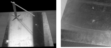
Figure 2 Antenna measurement bench.
At this point, it is still difficult to validate a tag since the connection between the chip and the antenna introduces a supplementary resistance and capacitance that are hard to characterize. The final goal, however, is a tag that is suited to an application. So the next important characterization is to be able to read a tag with an RFID reader. This setup means that all constraints are included in the measurement. Modern readers can be programmed to the needs of the user, so we are working with different types of reader to develop first level software. This software provides the basic functions of reading and writing but with the choice of the user on the frequency band to test. In this way, it is possible to measure with an accuracy of a few hundreds kilohertz the position of the resonance frequency. This proves enough for the practical design of passive tags.
From the ability to read tags properly we are developing a reading distance bench that will allow for various measurements. The first goal is to be able to measure the maximum distance from which a tag can be read by a given reader. It is then possible to reconstruct a 3D radiating pattern of the tag, even if it is not based on electromagnetic field strength measurements. This pattern will help to validate the tag design at the field level. Of course, this setup should be free from metals so as to allow for only taking into account the tag. The second level is to put up an environment around this measurement bench and place the tag onto an object. The possibilities for characterizing the tag in a real environment will then provide many interesting experimental data for designing better tags.
3. Achievements
3.1. Simulated tags
The first phase of design was actually focused on mastering the simulation software based on a standard design provided by our partner in France (LCIS, Pr. Smail Tedjini). This design, shown in figure 3, is a narrow band UHF antenna already designed for compatibility with the STMicroelectronics XRAG2 UHF chip. The interest in studying this tag lies in the possibility of studying the accuracy provided by Microwave Studio based on a known design.
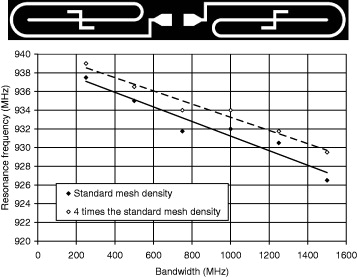
Figure 3 LCIS antenna design (930 MHz) and mesh density impact on resonance frequency.
The resonance frequency of an antenna can be obtained roughly with a coarse mesh. But when it comes to optimization, it is important to know how the mesh density influences the simulated resonance frequency. We varied the mesh density in our simulations related to the metal layer (local mesh). We noticed that increased by a factor of 4 the in-plane mesh density increases the resonance frequency by about 1–3 MHz. Furthermore, we varied the bandwidth of the input signal sent to the port connecting the two arms of the dipole antenna. As seen in figure 3, this parameter in the simulation influences the computed resonance frequency. The variation is of the order of 10 MHz for an input signal bandwidth from 250 MHz to 1.5 GHz. The lines on the figure are linear regressions over the simulated data.
The observed variations will have no impact on the design of a broadband tag since the variation in the resonance position is of small significance. The ongoing design process for a broadband tag is therefore not impacted by such an influence in the simulation parameters. But this is not the case for the narrow band type UHF tag, where the resonance should be well simulated to match the real conditions. Such tags are aimed at specific applications where the narrow band acts as a filter when reading a tag in a given frequency band. This specific point will be studied to provide a stable design environment for complete UHF tag simulation at LNT.
3.2. Passive tag on PET
In the present state of the process, a 4'' square PET substrate is carefully cleaned using a combination of wet and dry cleaning (RIE with oxygen plasma). The chips are then placed on the PET prior to antenna fabrication. Squares of the size of the chip are cut in the substrate and the chips are placed so as to be flat with the PET surface. Then a drop of epoxy glue is deposited and cured to maintain the chip in position [10]. In this situation, the contact pads of the chip are at the same level as the PET surface. This makes it easier to process this important part of the tag in the subsequent step.
This substrate is affixed to a holder in order to maintain its plane state in the subsequent process steps. Then it is subjected to copper sputtering (Leybold Univex 350 monochamber) to obtain a high quality copper thin film. As temperature is a criterion for the safe processing on PET [9], the sputtering dc power is set at 40 W. Then the patterning process is realized using a dry film photoresist. This film is laminated using a standard laminator, as shown in figure 4. Then it is exposed through a flexible mask in order to pattern the antenna and the connections with the chip in a single lithography step. Most dry film photoresists being negative, special care is taken to ensure a good patterning process.
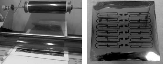
Figure 4 Lamination process and after development of the photoresist (antenna alone).
The photoresist is then developed in an alkaline developer. At this stage, it is still necessary to remove the copper from the different parts exposed. This is done by wet etching in an aqueous solution of H 2 SO 4 (1.3 mol l −1) and K 2 Cr 2 O 7 (0.63 mol l −1), which provides an etching rate of 5 nm s −1. The obtained tags are shown in figure 5.
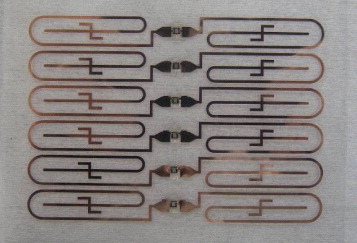
Figure 5 Completed tags with connection pads.
Opposite to using liquid photoresist, this process does not require spinning with all of the related problems of polymer films. The main drawback is a decreased accuracy of the pattern, which is in the range of a few tenths of microns. In the case of an RFID tag, this variation can be reduced by engineering the mask and decreased to a level small enough to be compatible with the applications. On the other hand, the quality of the connection is improved compared to the use of liquid photoresist because the lift-off step is avoided. This step is believed to bring difficulty to maintain adhesion between the copper thin film and the polymer substrate and other plastic parts (epoxy glue and chip packaging).
At this stage, the tags are connected but the antenna metal is not thick enough. For maximum electromagnetic field penetration in copper in the UHF band, a minimum metal thickness of 4.5 μm is required at the bulk resistivity of copper. A safe assumption calls for a 7–10 μm thick copper antenna, which is not reachable via the sputtering process alone. Therefore, we are engaged in the adaptation of copper electrochemical deposition onto our tags to reach the proper thickness for functional tags. Even though very well known and optimized for the PCB industry, we have to properly adjust the processing parameters in order to achieve homogeneous highly conductive copper thick film for our tags.
3.3. Tag reading
Modern RFID UHF readers provide many functionalities to interact with the tags. Using a USB reader from IDTronic, Germany, with a reading range of up to 1 m, we developed a first level software to perform our experiments. The interface shown in figure 6 illustrates the different functions for interacting with the tag: reading, writing, of course, and also frequency selection. This last feature is based on ETSI protocol with 200 kHz spaced channels. The user is able to select from 2 to 10 consecutive channels in the full frequency range of 860–960 MHz. This allows for scanning the entire frequency band in order to test the tag with a rather good accuracy.
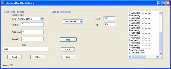
Figure 6 Successful reading of fabricated tags.
Figure 6 illustrates the successful reading of fabricated tags (thin copper antenna) at short distance. The chosen design was at 930 MHz and the obtained resonance frequency was at 953 MHz. Firstly, it validates the fabrication process in terms of electrical connection between the antenna and the chip. Secondly, the resonance frequency difference validates the tag because an antenna with a thickness below the skin depth will experience a shift towards higher resonance frequency.
4. Outlook
This paper reviews the structure of the RFID platform and some of the present achievements in RFID tag developments at LNT. The emphasis at this stage is on stabilizing the fabrication process details for obtaining a fully functional tag on polymer film. The final electrochemical deposition step is under optimization and will complete the process flow. The next developments will then contribute to lower the cost and provide flexibility to address different substrates, especially at the connection level.
On the design side, the primary goal is to reach a broadband tag, which has a lot of important applications in the field of logistics. This work includes the continuous exploration of the capability of the simulation software for these specific electromagnetic structures that are RFID tags.
Finally, we have started engaging in the measurement and characterization of the properties of the fabricated tags in order to close the loop and obtain valuable information for the optimization of the tags in the context of well understood fabrication process flow.
Acknowledgments
The financial support of the Ministry of Science and Technology is acknowledged. Pr Tedjini (Laboratoire de Conception et Intégration des Systèmes, Grenoble-INP, Valence, France) provided one of the antenna designs. We also want to acknowledge the technical support of CST for helping our progress on simulations using Microwave Studio.