
Abstract
This research presents the deposition and device fabrication of epitaxial Pb(Zr,Ti)O3 (PZT) thin films for applications in microelectromechanical systems (MEMS). A piezoelectric micro-membrane is described as an example. Using the pulsed laser deposition (PLD) technique and the MEMS microfabrication process, the piezo-membranes with diameters ranging from 200 to 500 μm were obtained. The displacement of piezo-membranes increased from 5.1 to 17.5 nm V−1 with a piezoelectric-membrane diameter in the range of 200–500 μm. Furthermore, the effect of PZT film-thickness on the mechanical properties has been investigated. By using the conductive-oxide SrRuO3 (SRO) layers as the electrodes, the degradation of both ferroelectric and piezoelectric properties is prevented up to 1010 switching cycles.
Export citation and abstract BibTeX RIS

Content from this work may be used under the terms of the Creative Commons Attribution-NonCommercial-ShareAlike 3.0 licence. Any further distribution of this work must maintain attribution to the author(s) and the title of the work, journal citation and DOI.
1. Introduction
Thin film processing is quite important for development of the miniaturization of electronic devices with low operating voltage. Epitaxial growth of PZT thin films on a silicon substrate is considered to be a key technology for fabricating the thinner and smaller electronic devices, because their leakage currents are expected to be lower than those of polycrystalline films [1, 2]. Furthermore, epitaxial PZT films also exhibited better ferroelectric and piezoelectric properties than polycrystalline PZT films [3].
Moreover, thin film processing techniques have been receiving much attention for applications in piezo-MEMS devices, such as biosensors, micro-pumps and micro-machined ultrasonic transducers (MUTs). In comparison with other common deposition techniques, like sputter deposition [4, 5], evaporation [6, 7], metalorganic chemical vapor deposition (MOCVD) [8, 9] and sol–gel processing [10, 11], the PLD technique offers some advantages. Most important is its ability to transfer material stoichiometrically from a multicomponent target to a growing film. This is very important for complex oxides such as PZT, because their physical properties strongly depend on the precise control of the chemical composition. Second, PLD is a promising technique for thick film fabrication because it offers the advantage of a high deposition rate. Because of the high deposition rate in the pulse, moreover, the mass transfer from the ablation plume to solid thin films is improved. This allows deposition at high growth temperatures, especially for the epitaxial growth of volatile materials. In the case of PZT thin film deposition, it results in a less significant loss of the more volatile elements, like lead (Pb).
The aim of this work is to investigate the piezoelectric and ferroelectric properties of the PZT grown on silicon membranes using SrRuO 3 (SRO) layers as the top- and bottom-electrodes. Furthermore, the effects of membrane geometry and oxide-electrodes are discussed.
2. Experimental procedure
2.1. Membrane fabrication
Figure 1 shows the flowchart of the piezoelectric PZT membrane fabrication process. Devices were fabricated on a (100) Silicon-on-Insulator (SOI) wafer with a 5-μm-thick silicon layer and a 2-μm-thick SiO 2 buried oxide (BOX) layer, as shown in figure 1(F1). The silicon-membrane was fabricated using deep reactive-ion etching (DRIE) from the backside of the wafer. The BOX layer that acts as an etch stop in the DRIE process is then removed by buffered-hydrofluoric acid (BHF) (figure 1(F2)). The resulting thickness of the Si-membrane was 5 μm. Then, the pre-patterned SOI wafer was cut into substrates with dimensions of 20×20 mm 2. These are called pre-patterned SOI substrates. The device is over an area of 10×10 mm 2 at the center of the pre-patterned SOI substrate.
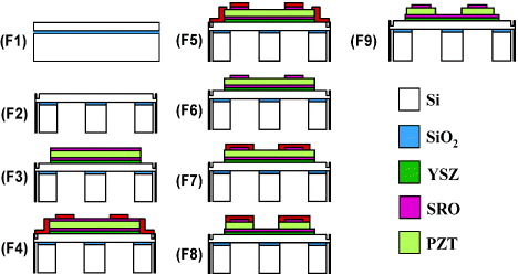
Figure 1 Fabrication process of the piezoelectric PZT film membrane on pre-patterned SOI substrates.
The deposition of a multilayer SRO/PZT/SRO/YSZ began with the deposition of a 100-nm-thick Yttria-stabilized zirconia (YSZ) buffer-layer on top of the SOI. The YSZ buffer-layer acts as a barrier layer against lead diffusion during PZT film deposition and prevents the formation of an excessive SiO 2 amorphous layer on the surface of the Si substrate. Moreover, it also acts as a crystallization template for the piezoelectric stack, allowing epitaxial layer growth.
Next, a 100-nm-thick SRO electrode and a 1-μm-thick PZT layer were deposited. Deposition of the piezoelectric stack was completed with a 100-nm-thick SRO top electrode layer deposition (figure 1(F3)). All layers in the piezoelectric stack were deposited by pulsed laser deposition. Details of the optimal deposition conditions of the multilayer stack were published previously [12, 13].
Figures 1(F4)–(F9) show the fabrication of piezoelectric membranes by the MEMS microfabrication process, including photolithography and etching. First, the top SRO layer was etched by Ar-ion beam etching (steps F4 and F5). Next, the PZT film was removed by sequential wet-etching with HF and HCl solutions (steps F7 and F8). The top-view structure of the membranes is shown in figure 2 after release of the photoresist layer (figure 1(F9)).
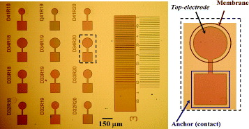
Figure 2 Microscope images (top-view) of the fabricated membrane arrays with the top-electrodes of 100–160 μm in a 200-μm-diameter silicon membrane.
In fabricating a PZT thin film membrane actuator, silicon residues may result from an uneven etch rate while releasing the membrane from the SOI substrate. The silicon residues can reduce the effective area of the membrane, and then decrease the properties of the actuator. Figure 3(a) shows an SEM image of the backside of a PZT thin film membrane actuator. The membrane is uniform in thickness and without any residue appears circular in shape. This indicates that the diameter of the fabricated membrane actuator is corrected with that of the membrane design. The surface and deflection profiles of a 200-μm-diameter circular-membrane, measured using a white-light interferometer, are shown in figure 3(b). Without applying bias voltage, the upward bending of the piezoelectric membrane results from built-in gradient tensile stress between the PZT thin film and the silicon membrane.

Figure 3 (a) SEM images of the backside view and (b) measured membrane deflection (or initial bending) of a fabricated PZT thin-film membrane actuator.
2.2. Characterization methods
The polarization hysteresis (P–E) loop was measured at ±200 kV cm −1 amplitude and 1 kHz frequency, using a ferroelectric film test system (TF 2000 Analyzer). A Süss MicroTech PM300 manual probe-station equipped with a Keithley 4200 Semiconductor characterization system is used for the capacitance measurement. The capacitance–electric field (C–E) was performed using an ac signal of 1 kV cm –1 and a 10 kHz frequency with the dc bias sweeping from −200 to + 200 kV cm −1 and then back to −200 kV cm −1. The corresponding dielectric constant was calculated from this C–E curve. The orientation of the film was observed by high-resolution x-ray diffraction (XRD, Bruker D8 Discover) with a Cu-Kα cathode in the Bragg–Brentano geometry.
The Polytech MSA-400 micro system analyzer is used for the analysis and visualization of structural vibration and surface topography in microstructures such as membranes and MEMS devices in general. Full integration of a microscope with a scanning laser Doppler vibrometer (LDV) was carried out for measurements of the actuation of membranes.
3. Results and discussion
3.1. Structure and ferroelectric properties of membranes
From x-ray diffraction (XRD) (not shown here), the PZT films that were grown on SRO/YSZ/Si substrates had a (110) orientation. As shown in the phi-scan plots [13], the rotation angle phi-scan (ϕ) of the (202) peak of YSZ coincides with that of Si. Moreover, four identical sets of SRO(002) peaks are positioned around the reflections corresponding to Si(202). Since the SRO(002) peak is divided over two peaks situated at + 10° and −10° with respect to Si, this means that twin domains exist in the thin film. These results indicate that the cube-on-cube epitaxial orientation relationship with the substrate is obtained for all YSZ, SRO and PZT layers, described by (110) PZT/(110) c SRO/(001) YSZ/(001) Si [14].
The ferroelectric properties for the PZT film membranes were characterized using polarization and dielectric constant measurements, as shown in figure 4. The remnant polarization P r was measured as 18.6 μC cm −2 and the dielectric constant calculated from the capacitance measurement was 1360.
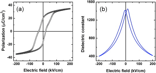
Figure 4 (a) Polarization hysteresis (P–E) loop and (b) dielectric constant (ε–E) curve for the PZT film membrane after device fabrication. The P–E loop was determined at ± 200 kV cm −1 amplitude and 1 kHz frequency while the dielectric constant curve was measured using an ac signal at 1 kV cm −1 and 10 kHz frequency.
3.2. Electromechanical behavior
The LDV technique was used to measure the electromechanical behavior (displacement) of the membranes actuated with a sinusoidal voltage. Membrane displacement was measured at 6 V p–p (peak-to-peak) amplitude and 8 kHz frequency (well below resonance). Figure 5(a) shows a typical piezoelectric vibration response of a membrane of 200 μm diameter. The laser scanning area covered both the top electrode and the surrounding PZT film. To investigate the effect of membrane geometry on membrane displacement, the measured central displacements for PZT membranes with various diameters are illustrated in figure 5(b). The displacement increases from 5.1 to 17.5 nm V −1 when the diameter is in the range of 200–500 μm. The top-electrode size is roughly 60% of the diameter of the membrane.

Figure 5 (a) Upward-displacement of the 200-μm-diameter membrane, which was carried out at 6 V p–p amplitude and 8 kHz frequency (off-resonant conditions). (b) Plot of the measured central displacement as a function of the diameter of the membrane.
The effect of the actuation voltage amplitude on the 200-μm-diameter membrane was evaluated by applying a sine wave signal of an ac-voltage between 1 and 6 V p–p (peak-to-peak) at a frequency of 8 kHz. The results, shown in figure 6(a), indicate that the displacement was proportional to the applied voltage.
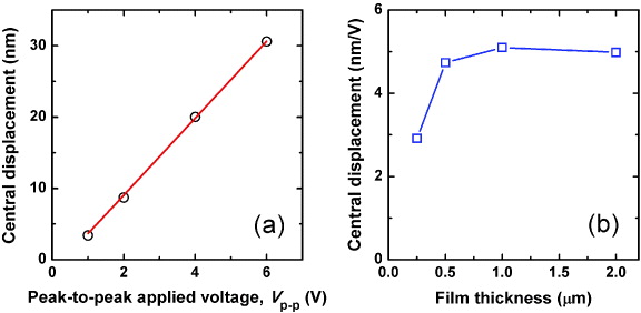
Figure 6 Membrane central displacement as a function of bias applied voltage (a) and PZT film-thickness (b) for the membrane of 200 μm in diameter.
Figure 6(b) illustrates that the displacement of the 200-μm-diameter membrane increased from 2.9 to 5.1 nm V −1 with film thickness in the range of 0.25–1 μm and slightly decreased for the thicker films (1–2 μm). Like the polarization property, in the range of 0.25–1 μm film thickness, this variation in the piezoelectric property was attributed to the interfacial layer at the film/electrode interface. With increasing film thickness, the effect of the interfacial layer is decreased, thus leading to a large d33 coefficient of PZT thin films. A slight decrease in the displacement with the thicker films (1–2 μm) is observed, because the PZT films get softened at these films [15].
Polarization fatigue is responsible for the decrease in the displacement of the PZT/Pt piezoelectric stacks with increasing switching cycles [16]. This problem can be solved by using conductive-oxide SRO electrodes in the piezoelectric stack [15]. The SRO electrodes can reduce or prevent the accumulation of oxygen vacancies near the PZT/SRO interface by changing its oxygen non-stoichiometry. No decrease in the remnant polarization was hence observed in the PZT/SRO capacitors with increasing switching cycles. Figure 7 reveals the phenomenon of displacement of the 200-μm-diameter membrane as a function of working cycle. It is noted that the displacement fatigue did not occur up to 1010 cycles.

Figure 7 Remnant polarization and displacement as a function of the number of working cycles of the 200-μm-diameter membrane. The polarization was carried out using a bipolar switching pulse of 200 kV cm −1 pulse height and 5 μs pulse width, and was measured at ± 200 kV cm −1 and 1 kHz. The piezoelectric displacement was carried out at 6 V p–p amplitude and 8 kHz frequency.
4. Conclusion
We have demonstrated the behavior of PZT thin film as an integrable actuator in MEMS technology. Piezoelectric membranes based on epitaxial PZT thin films grown on silicon membranes were designed and analyzed successfully. Using SRO layers as the top- and bottom-electrodes allowed the use of typical wet and dry etching processes, thus permitting a design based completely on standard microfabrication processes. The good quality, crack-free membrane is mechanically strong enough to support the ferroelectric micro-sensors, which may have each element size in the range of 200–500 μm. Membranes actuated by the PZT thin films show deflection of several nanometers and these make possible the use of this kind of actuators for resonant actuator applications, as in accelerometers.
Next, the effects of membrane geometry on the piezoelectric displacement were investigated. The displacement increased with an increase in the membrane diameter. Furthermore, the piezoelectric membranes with conductive-oxide SRO electrodes showed neither polarization nor actuation fatigue up to 1010 cycles, which clearly indicates that the piezoelectric PZT film membranes can work stably for a long period of time. As a result, the SRO/PZT/SRO thin-film stacks have great potential to serve as sensors and actuators for many MEMS applications.
Acknowledgments
The authors gratefully acknowledge the support of the Smart-Mix Program (Smart-Pie) of The Netherlands Ministry of Economic Affairs and The Netherlands Ministry of Education, Culture and Science, as well as the Vietnamese Overseas Scholarship Program (MOET-VOSP Project 322).