
Abstract
This study applied an in situ electric contact resistance technique to monitor delamination induced by indentation loads. A suddenly increasing indentation depth, together with a simultaneous drop in monitoring contact current, suggests that delamination occurred. During unloading processes, the rapid decrease in both contact depth and current imply that the delaminated film was suspended as long as the indentation load became sufficiently small. When delamination occurred during oscillating processes, the contact current was found to drop from an initial value to a steady value, which is related to a loss of interfacial contact.
Export citation and abstract BibTeX RIS

Content from this work may be used under the terms of the Creative Commons Attribution-NonCommercial-ShareAlike 3.0 licence. Any further distribution of this work must maintain attribution to the author(s) and the title of the work, journal citation and DOI.
1. Introduction
With the development of the microelectronic and microelectro-mechanical system industries, the technologies of coating films are playing an increasingly important role. Because indentation load-depth curves were used to determine the mechanical properties of materials, the depth-sensing indentation test has become a popular and powerful tool for determining the mechanical properties of bulk specimens [1–5] or thin film/substrate systems [6–8]. For semi-conductive materials, in-situ electric contact resistance measurement was proposed to detect phase transition induced by indentation stress [9]. Dynamic indentation tests can induce interfacial fractures and damage due to fatigue failure [10–11]. An initial interfacial crack is created when the applied indentation load reaches a critical value, then interfacial adhesion energy can be evaluated by analyses of recorded indentation results [12, 13] together with observations of delamination length, which require post measurements. Regarding a pop-in event, in which penetration depth suddenly increases under an almost invariant load, as a sign of delamination, Wei et al [14] considered that the slope of the force-depth data at the end of unloading processes is related to the deflection of the suspended film. However, the relation between pop-in and delamination remains unclear. In this study, the in-situ electric contact resistance technique was applied to clarify the relation. Then, a simultaneous occurrence of pop-in and current drop can be used as a delamination signal.
2. Experimental
In order to detect delamination occurring during indentation tests, quasi-static and oscillating experiments were performed on a TriboScan system (Hysitron, US) with a conductive Berkovich indenter, as shown in figure 1. An as-deposited Ti x N y film with a thickness of 500 nm, which was sputtered on a SKD61 tool steel substrate, was chosen for delamination by nanoindentation techniques. For quasi-static experiments, the load schedule was arranged to consist of a loading segment (loading rate of 10 μN s −1), a hold segment (constant load of 10 mN for 10 s), and an unloading segment. For oscillating experiments, the load schedule consists of a loading segment, a partial-unloading segment (unloading rate of –10 μN s −1 to 5 mN s −1), a sinusoidal cyclic-oscillating segment (load amplitude of 2.5 mN at 1 Hz for 100 cycles), a final-unloading segment (unloading rate of –10 μN s −1), and three hold segments (10 s), which are used to buffer deformations due to the prior processes. It should be noted that the constant load during the first hold segment is the maximum load.
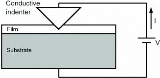
Figure 1 This scheme demonstrates the indentation experiment using a conductive diamond indenter. The setup allowed us to monitor electric contact resistance and to detect changes in the interfacial conditions during penetration of the indenter.
3. Results and discussion
3.1. Pop-in events occurring during processes
A pop-in event is observed to be the sign of indentation-induced delamination [13]; one typical result is shown in figure 2.
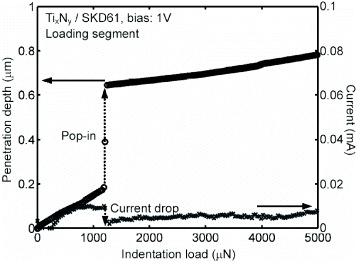
Figure 2 Typical loading result of in situ contact current measurement, which demonstrates the simultaneous occurrence of the current drop and pop-in event during the loading process. The presented data are not the entire loading results.
A significant pop-in event occurred at approximately 1200 μN, and the penetration depth jumped from 0.19 μm to 0.68 μm. At the same time, a corresponding contact current drop was found. In general, the contact current approximately increases with contact load due to the increase in contact area. At small loads (<200 μN in figure 2), the current results were found to fluctuate around zero; this should be related to multiple (summit) contacts. After that, the current rose to around 0.01 mA and remained for a while before pop-in occurred. In the load range of 500–1200 μN, the depth data increased with load and remained almost constant; this should be a sign of structural change of the film/substrate interface. And after pop-in occurred, both the penetration depth and the contact current approximately increased with applied load. Compared to the load-depth data before pop-in occurred, penetration increased much more slowly. This seems reasonable since the increase in penetration depth (due to pop-in) makes indentation more difficult.
3.2. Unloading results after pop-in events
After delamination, the unloading results reveal a two-stage behavior divided by an elbow, where the debonded film was just in contact with the substrate. When applied load is large enough, part of delaminated film is still in contact with the substrate due to elastic recovery. In this case, greater contact stiffness is found. On the other hand, the debonding film will be fully suspended if the applied load decreases to a sufficiently small limit. A typical unloading result with a two-stage behavior was shown in figure 3, where the elbow was found to be 3500 μN. Similar to the depth data, the current data showed approximately two-stage behavior with the same load of elbow. The good agreement between depth and current data suggests that the in-situ electric signal can supply complementary information of sub-surface.

Figure 3 Typical unloading result of in situ contact current measurement after a pop-in event occurred during loading process. The two-stage behavior suggests the delaminated film is suspended as long as the indentation load is sufficiently small. The elbow indicates a just contact between the delaminated film and substrate.
3.3. The relation between current results and delamination
Experimental contact resistance comes from complicated sources; therefore, it is difficult to quantitatively analyze contact current results. However, the impedance can be simplified into two types: bulk and junction. In this study, the total resistance is considered as the scheme shown in the left portion of figure 4(a). The resistors R I/F , R F/Sn represent the impedance due to indenter/film and film/substrate junctions, and those R Fn represent the impedance due to conducting in the film, where n=1–3 denote primary, secondary and tertiary deformation zones. The primary deformation zone, which marked by dark background in figure 4, is bounded by the permanently deformed region of the substrate interface; the secondary deformation zone, which marked by light background in figure 4, means the delaminated region; and the tertiary deformation zone is other region. The delaminated zone is assumed to be larger than the primary deformation zone, and buckling is assumed to occur since a compressive residual stress exhibited in the film. It should be noted that the three deformation zones cannot be precisely defined and the resistances of those resistors are not constant. Here other sources of impedance, such as conducting in the indenter and the substrate are neglected.
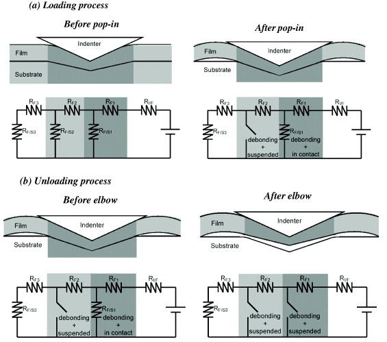
Figure 4 (a) For the pop-in event during loading process, the current drop is resulted from delamination of the film and thus a loss of interfacial contact. (b) Due to suspension of the delaminated film during the unloading process, both of the contact depth and current decrease rapidly after the elbow.
As shown in the right portion of figure 4(a), after pop-in occurred, the resistor R F/S2 turned into a breaker since in the secondary deformation zone the film is no longer in contact with the substrate. This is believed to be the main contribution to the increasing total resistance. During unloading processes, the resistors should be function of applied load because the strain condition of film and the contact conditions of junctions are changing. When the applied load went smaller than the elbow value, the elastic recovery of the substrate was finished and thus the delaminated film was fully suspended over the substrate. Therefore, the resistor R F/S1 eventually turned into a breaker and the total resistance behavior changed. It is reasonable for that both the depth and current results have similar two-stage behaviors and the same elbow value.
3.4. Pop-in events occurring during oscillating processes
Not only in loading processes, pop-in events occur also during oscillating processes; and then two-stage behaviors were exhibited. For the case presented in figure 5, a significant pop-in occurred at cycle No. 11 and the penetration depth at the maximum load jumped approximately from 1.05 μm to 1.15 μm; and the contact current was found to drop from 7.8 μA to 5.1 μA. After that, both depth and current data stayed in their steady values till the end of the oscillating process. The variation of depth together with current would be regarded as a state change during delamination. It indicates that all the indentation-induced strain energy has turned to surface energy and a relatively steady state was established from cycle No. 12 to No. 100.
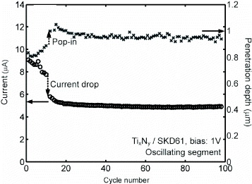
Figure 5 Typical oscillating result of in situ contact current measurement without any pop-in event occurred during loading process. Both of the current drop and pop-in event occurred during cycle No. 11.
4. Conclusion
This study proposed an application for monitoring indentation-induced delamination of a conductive or semi-conductive film/substrate specimen. When a pop-in event together with a current drop signal is observed, delamination occurs. This detecting technique is found to be applicable in quasi-static and dynamic oscillating experiments. The correlation between a pop-in (depth jump) event and the simultaneous current drop proves occurrence of delamination previously assumed. In summary, in-situ electric current results can provide complementary information for detecting delamination. It seems that an increasing penetration together with a non-increasing current can be used to be a pre-delamination sign.