
Abstract
Bulk heterojunction organic solar cells were fabricated by sandwiching the active layer between indium tin oxide (ITO) and Al electrodes. The active layer used was a blend of poly(3-octylthiophene-2,5-diyl) (P3OT) as the electron donor and (6,6)-phenyl C71 butyric acid methyl ester (PC71BM) as the electron acceptor. The active layer thin films were deposited by an inkjet printing technique. Prior to deposition of the thin films, the active materials were blended in three different solvents. The printed films were annealed at three different temperatures. It was found that the selection of the appropriate solvent and annealing treatment significantly influences the printing process, the morphology of the printed film and subsequently the performance of the solar cell devices.
Export citation and abstract BibTeX RIS

Content from this work may be used under the terms of the Creative Commons Attribution-NonCommercial-ShareAlike 3.0 licence. Any further distribution of this work must maintain attribution to the author(s) and the title of the work, journal citation and DOI.
1. Introduction
The organic solar cell is a promising candidate for a low-cost renewable energy source [1–3]. In order to obtain mass production, plus large scale and flexible organic photovoltaic cells, there are several deposition methods that are being intensively developed and the inkjet printing technique shows significant potential to achieve this goal [4]. However, film formation by inkjet printing is fundamentally different from the printing process in terms of the jetting of droplets, and the interaction among the droplets plays a key role in obtaining high-quality printed film. In terms of device architecture, the bulk heterojunction type has become the most popular device [5]. In the bulk heterojunction structure, the donor and acceptor materials are simply blended as one solution, deposited as the active layer and then sandwiched between two electrodes.
In this work, the active layer used was composed of blended poly(3-octylthiophene-2,5-diyl) (P3OT) and (6,6)-phenyl C 71 butyric acid methyl ester (PC 71 BM). The P3OT:PC 71 BM pairing was selected for the following reasons. P3OT is a long alkyl side chain polymer that is expected to produce high-quality thin film. Hence, it may produce a high photovoltaic performance in solar cell structures. Meanwhile, PC 71 BM is a high optical absorption acceptor material in the visible range. The combination of both materials is expected to give a reasonably good photovoltaic performance.
Prior to the deposition process of an organic thin film by the inkjet printing technique, the chemical should be prepared in the form of ink by dissolving it in a particular solvent. The choice of solvent may affect the quality of the film. This paper reports a study on the effect of using three different solvents on the quality of the printed organic solar cells' active layer films. The quality of the films was examined based on the morphology and the performance of fabricated bulk heterojunction organic solar cells. At the end of the deposition process, the solvent must be removed from the printed film. This was done through an annealing treatment that was also performed in a vacuum oven at various temperatures and for different periods. The three different solvents used were a mixture of chloroform/dichlorobenzene, dichlorobenzene and a mixture of dichlorobenzene/mesitylene. It was found that the selection of solvent is a critical part in the formation of printed film and is closely related to the physical properties of the solvents, such as vapor pressure, boiling point and surface tension. The surface morphology of the printed films was significantly effected by the formation process and the drying process of the films.
2. Experimental
The organic materials used in this experiment were poly(3-octylthiophene-2,5-diyl) (P3OT) and (6,6)-phenyl C 71 butyric acid methyl ester (PC 71 BM) (Sigma Aldrich). These chemicals act as electron donor (D) and acceptor (A) materials, respectively. Both materials were dissolved in three different solvents and then mixed with the ratio of 1:1 (weight) while being maintained at a concentration of 2 wt% (26 mg ml −1). The solvents were a mixture of chloroform/dichlorobenzene (1:1), dichlorobenzene and a mixture of dichlorobenzene/mesitylene (2:1), namely solutions A, B and C, respectively. The blended solutions were stirred for 16 h at ambient temperature in air and were then ready to use as ink. Prior to printing, the optical properties of the blended solutions were observed by using the UV-Vis spectrophotometer (Perkin Elmer Lambda 900 UV-VIS/NIR Spectrometer). We also observed the wettability of the solution on ITO-coated glass substrates by measuring the contact angle by using a contact angle geniometer.
The blended solutions were deposited on indium tin oxide (ITO)-coated glass substrates (20 Ω sq −1) by using a commercial piezoelectric inkjet printer (Dimatix Material Printer (DMP 2800 system)). The printer was placed in a glove box with an argon atmosphere. The substrates were placed 1 mm below the inkjet printhead and the typical waveform settings used a voltage between 14 and 16 volts with a pulse width of 20.2 μs. The printed films were then left to dry in a Petri dish until the color of the films changed from orange to purple. Post-deposition heat treatment was carried out by annealing in the vacuum oven at various temperatures and for different periods, i.e. 120 °C, 140 °C and 160 °C for 30 and 60 min. The surface morphology of films was characterized by atomic force microscopy (CP-II Veeco) using tapping mode.
The films were then used as the active layer of bulk heterojunction organic solar cells. The active layer was sandwiched between ITO and the aluminum cathode, as shown in figure 1. The aluminum thin film was deposited through a shadow mask by the electron gun evaporation system. The photovoltaic performance of the solar cell devices was studied by current–voltage measurements (Keithley SMU 237) both in the dark and under AM 1.5 (Newpoint Solar Illumination) with an intensity of 100 mW cm −2 in the air.
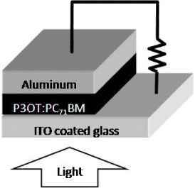
Figure 1 Bulk heterojunction organic solar cell structure.
3. Results and discussions
The UV-Vis optical absorption spectra of blended P3OT:PC 71 BM solutions in three different solvents, i.e. a mixture of dichlorobenzene/chloroform (DCB/CHL), dichlorobenzene and a mixture of dichlorobenzene/mesitylene (DCB/MST), are shown in figure 2. All of the solutions showed almost similar absorption spectra in the range of 300–700 nm. The examined contact angles of all of the solutions on ITO-coated glass substrates were less than 10°, which indicated good wettability.
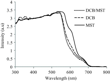
Figure 2 UV-Vis absorption spectra of blended P3OT:PC71BM solution with three different solvents.
The blended solutions were inkjet printed onto the ITO substrates. Figure 3 shows images of the films examined by digital microscope (National DC3-163) with a width of 4.5 mm. At a glance, these films exhibit different structures for different solvents. For the chloroform/dichlorobenzene solvent (solution A), the solution was ejected with partial clogging at the nozzle orifice. This reduced the volume and velocity of some droplets and also changed the direction of the flying droplets. As a result, from this non homogeneous solvent, droplets were formed and caused many pinholes in the film (figure 3(a)). This problem may be due to the rapid evaporation of chloroform at the orifice of the nozzles, which left an accumulation of dry solute to block the droplet jetting process. In the case of the solution using pure dichlorobenzene solvent (solution B), jetting of the solution was controllable but produced an uneven film thickness (figure 3(b)). The drying process of solution B after printing is slow so that the printed ink may move to other parts to produce an uneven surface. As shown in figure 3(c), the quality of the printed film was improved by adding mesitylene into dichlorobenzene (solution C).
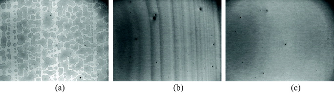
Figure 3 The blended P3OT:PC71BM film printed on ITO-coated glass using solvent. (a) Dichlorobenzene/chloroform, (b) dicholobenzene and (c) dichlorobenzene/mesitylene.
The dependence of the quality of the printed films on the solvents may be related to the physical properties of solvents, such as vapor pressure, boiling point and surface tension, as summarized in table 1. Chloroform has a high vapor pressure (159 mm Hg), hence the evaporation rate of solution A is high. In contrast, pure dichlorobenzene (DCB), which has a low vapor pressure, made the solution dry slowly, and its high surface tension may make it difficult to form a uniform printed film. By adding mesitylene, which has a higher vapor pressure (1.20 mm Hg) and a lower surface tension than DCB solution, the evaporation rate and the surface tension of the solution C have moderate values, hence improving the uniformity of the printed film thickness.
Table 1. Vapor pressure, boiling point and surface tension of solvents.
| Chloroform (CHL) | 159 | 67 | 27.5 |
| Dichlorobenzene (DCB) | 1.20 | 180 | 37.0 |
| Mesitylene (MST) | 1.86 | 165 | 28.8 |
In the next part we only considered the films prepared using a mixture of dichlorobenzene/mesitylene as the solvent. The freshly printed film is wet because it contains an amount of solvent that has to be removed through an annealing treatment. In this work, the annealing process was carried out in a vacuum oven by variation of temperatures and time. In our first trial, we annealed the film at 120 °C for 120 min and the film remained wet. In the next trial, we increased the temperature up to 140 °C for 60 min. The film was partially wet, especially at the upper part. In our last trial, the temperature was increased to 160 °C for 30 min. It was then found that the film was completely dry.
All annealed printed films were then used as the active layer of solar cell devices by sandwiching them between the ITO and aluminum electrodes. The photovoltaic performance was studied through the current–voltage (I–V) measurements in the dark and under 100 mW cm −2 AM 1.5 solar illuminations. It was found that the device with annealing treatment at 120 °C did not show the photovoltaic effect. This may be due to the presence of solvent in the active layer, which prevented the generated charge carriers from drifting to the electrodes. The device that was annealed at 160 °C also showed no photovoltaic effect. Since the annealing temperature is relatively close to the melting point of P3OT, i.e. 190 °C, some of the P3OT molecules may have evaporated, leaving the active layer with holes and voids. Only the device that was annealed at 140 °C showed a photovoltaic effect (figure 4).
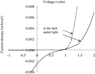
Figure 4 Current–voltage curve of printed solar cell device.
The I–V curves of the device in the dark showed diode behavior. The rectification ratio was calculated by comparing the current at ±2 V, while the series and shunt resistances were derived from the slope of the I–V curves in the dark at 2 V and 0 V, respectively. The rectification ratio, series resistances and parallel resistances of the device in the dark were 57, 167 and 2635 MΩ, respectively. The I–V curves of the devices under AM1.5 solar illumination showed the photovoltaic effect with poor diode behavior. The short current density was 2.3×10⁻³ mA cm −2, the open circuit voltage was 0.9 volts, the calculated fill factor was 0.145 and the power conversion efficiency was 3.3×10⁻⁴%. The generated photocurrent of the solar cell device obtained from this work is low for several reasons. Firstly, this is due to the existence of solvent in the active layer, which lowers the electrical conductivity of the film. Secondly, the microstructure of the inkjet printed films was poor, as indicated by the high surface roughness. The annealing process increased the average roughness of the film from 8.4 to 13.2 nm. The surface morphology of the printed films before and after the annealing treatment can be seen from the AFM images in figure 5. During annealing, the evaporated solvent left behind many voids, while the organic molecules did not have the ability to fill these voids. Work to overcome this problem is in progress, including improvement in the composition of solvent components and multiple temperature annealing treatment. Thirdly, the active layer thickness of 80 nm was smaller compared to the penetration depth of light in an organic semiconductor, which is typically of 80–200 nm. This might cause a small part of the photons to be effectively absorbed by the active material, thus exciton generation was reduced.
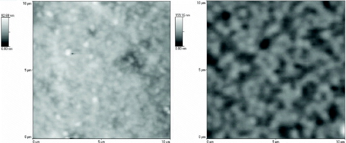
Figure 5 The AFM images of blended P3OT:PC71BM printed films (a) before and (b) after annealing treatment in a vacuum oven at 140 °C for 60 min.
The open circuit voltage obtained from this work is relatively high compared with those obtained from spin-coated devices. In our previous work, in which the film was prepared via spin coating, the open circuit voltage was 0.43 volt [6]. This difference may be related to the formation of the films. In inkjet printed film, the layer was deposited drop by drop where the donor and acceptor molecules were close together. In contrast, in spin-coated films, the donor and acceptor molecules were separated by a distance due to the centrifugal force during the spinning process [7]. Such close donor–acceptor separation may increase the electron hole dissociation probability, hence increase the V oc [8].
4. Conclusion
A selection of solvents and annealing treatments on blended P3OT:PCBM inkjet printed film as the active layer of bulk heterojunction solar cells has been investigated. A mixture of dichlorobenzene/mesitylene (2:1) as a solvent showed the best reliability in the printing process and the most homogenous printed film. The annealing treatment in a vacuum oven at 140 °C for 60 min succeeded in removing solvent but increased the surface roughness of the printed film.
Acknowledgments
The authors would like to thank the Malaysian Ministry for Higher Education and University Kebangsaan Malaysia for the research grants (UKM-RRR1-06-FRGS0002-2007, UKM-GUP-NBT-08-25-086 and UKM-OUP-NBT-27-120/2010).